
Samsung Semiconductor is charting a course toward Net Zero for Scope 1 and 2 by 2050, guided by our long-term strategic roadmap.
We are driving this transition through a dual approach: reducing direct emissions via advanced process and facility enhancements, and lowering indirect emissions by maximizing energy efficiency and expanding our renewable energy footprint.
Our vision extends beyond our own walls. By advancing our emission tracking systems and empowering our partners across the supply chain, we are systematically managing carbon footprints across the entire value chain—including Scope 3—to help every stage of our product's lifecycle contribute to reducing emissions across the value chain.
Samsung Semiconductor is charting a course toward Net Zero for Scope 1 and 2 by 2050, guided by our long-term strategic roadmap.
We are driving this transition through a dual approach: reducing direct emissions via advanced process and facility enhancements, and lowering indirect emissions by maximizing energy efficiency and expanding our renewable energy footprint.
Our vision extends beyond our own walls. By advancing our emission tracking systems and empowering our partners across the supply chain, we are systematically managing carbon footprints across the entire value chain—including Scope 3—to help every stage of our product's lifecycle contribute to reducing emissions across the value chain.
Samsung Semiconductor is charting a course toward Net Zero for Scope 1 and 2 by 2050, guided by our long-term strategic roadmap.
We are driving this transition through a dual approach: reducing direct emissions via advanced process and facility enhancements, and lowering indirect emissions by maximizing energy efficiency and expanding our renewable energy footprint.
Our vision extends beyond our own walls. By advancing our emission tracking systems and empowering our partners across the supply chain, we are systematically managing carbon footprints across the entire value chain—including Scope 3—to help every stage of our product's lifecycle contribute to reducing emissions across the value chain.
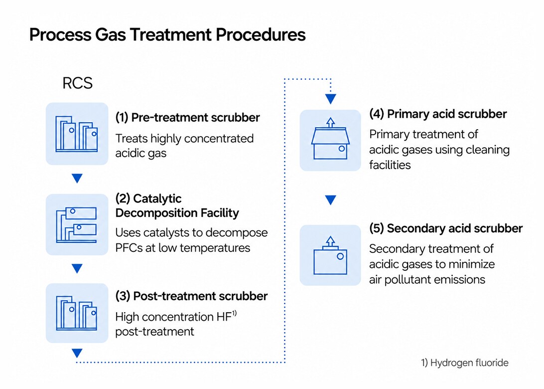
Samsung Semiconductor developed the RCS (Regenerative Catalytic System), the industry's first large-scale integrated process gas treatment facility, and has applied it across its production lines. In addition, the company has horizontally deployed its 3rd-generation catalyst—capable of achieving a PFCs1) treatment efficiency of 97%—to 25% of applicable systems, with plans to reach 100% deployment by 2026.
Samsung Semiconductor developed the RCS (Regenerative Catalytic System), the industry's first large-scale integrated process gas treatment facility, and has applied it across its production lines. In addition, the company has horizontally deployed its 3rd-generation catalyst—capable of achieving a PFCs1) treatment efficiency of 97%—to 25% of applicable systems, with plans to reach 100% deployment by 2026.
Samsung Semiconductor developed the RCS (Regenerative Catalytic System), the industry's first large-scale integrated process gas treatment facility, and has applied it across its production lines. In addition, the company has horizontally deployed its 3rd-generation catalyst—capable of achieving a PFCs1) treatment efficiency of 97%—to 25% of applicable systems, with plans to reach 100% deployment by 2026.
Samsung Semiconductor is continuously developing alternative gases with low Global Warming Potential (GWP), successfully replacing PFCs in several manufacturing processes. Since 2018, the company has deployed the C4F81) alternative (G1) and began the field application of G3 in 2025 to replace CF42), a major contributor to process greenhouse gas emissions. Looking ahead to 2026, Samsung Semiconductor plans to drive further reductions by introducing the CHF33) alternative (G2).
Beyond its own operations, we are committed to sharing these developed alternative gases with the wider industry, contributing to a collective reduction of carbon emissions across the entire semiconductor ecosystem.
Samsung Semiconductor is continuously developing alternative gases with low Global Warming Potential (GWP), successfully replacing PFCs in several manufacturing processes. Since 2018, the company has deployed the C4F81) alternative (G1) and began the field application of G3 in 2025 to replace CF42), a major contributor to process greenhouse gas emissions. Looking ahead to 2026, Samsung Semiconductor plans to drive further reductions by introducing the CHF33) alternative (G2).
Beyond its own operations, we are committed to sharing these developed alternative gases with the wider industry, contributing to a collective reduction of carbon emissions across the entire semiconductor ecosystem.
Samsung Semiconductor is continuously developing alternative gases with low Global Warming Potential (GWP), successfully replacing PFCs in several manufacturing processes. Since 2018, the company has deployed the C4F81) alternative (G1) and began the field application of G3 in 2025 to replace CF42), a major contributor to process greenhouse gas emissions. Looking ahead to 2026, Samsung Semiconductor plans to drive further reductions by introducing the CHF33) alternative (G2).
Beyond its own operations, we are committed to sharing these developed alternative gases with the wider industry, contributing to a collective reduction of carbon emissions across the entire semiconductor ecosystem.
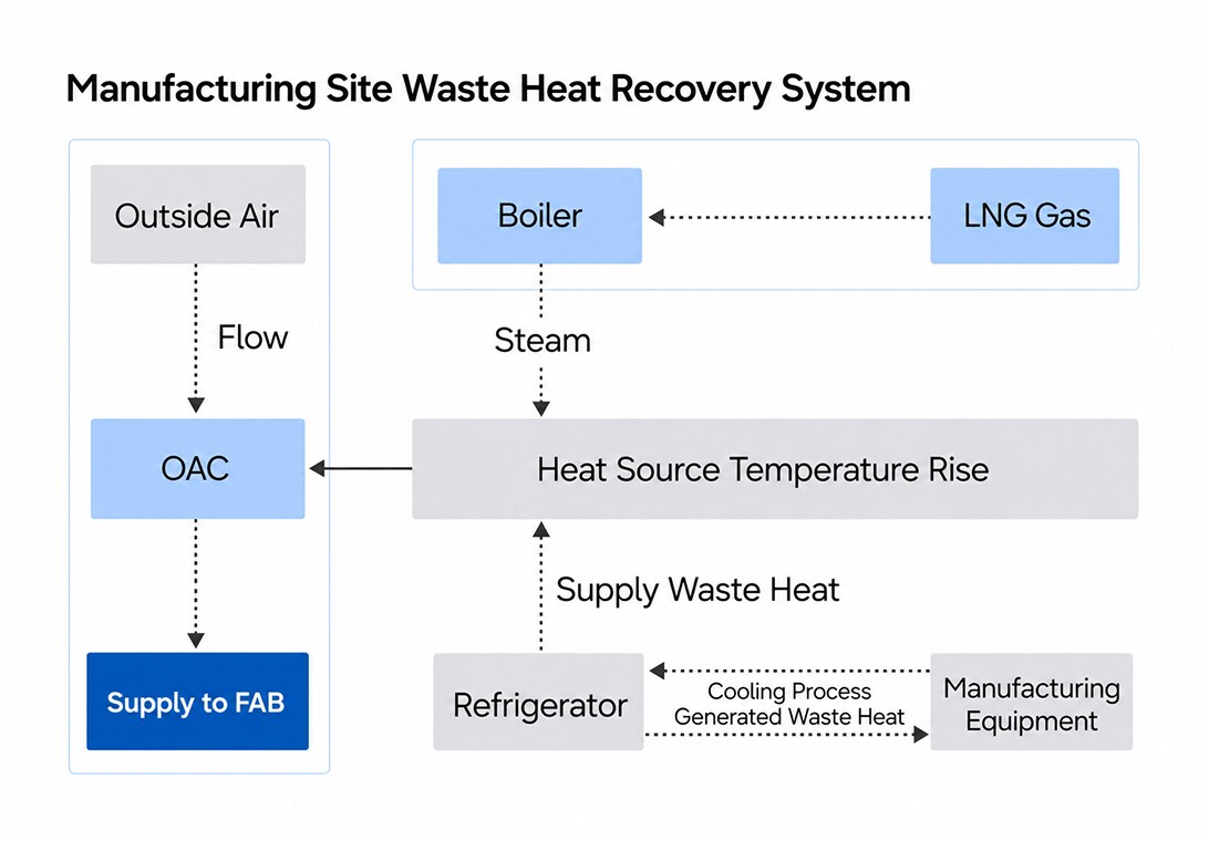
To reduce fuel consumption, Samsung Semiconductor is implementing a comprehensive strategy focused on process operation optimization, the introduction of non-fuel facilities, and the operation of advanced waste heat recovery systems. These recovery systems capture heat that would otherwise be discarded and repurpose it for outdoor air heating and hot water production, significantly reducing the usage of LNG.
As a result of these initiatives, the waste heat utilization rate at the Giheung, Hwaseong, and Pyeongtaek sites reached 55% in 2025. Samsung Semiconductor plans to expand these systems to existing production lines, further enhancing thermal energy efficiency across all business sites.
To reduce fuel consumption, Samsung Semiconductor is implementing a comprehensive strategy focused on process operation optimization, the introduction of non-fuel facilities, and the operation of advanced waste heat recovery systems. These recovery systems capture heat that would otherwise be discarded and repurpose it for outdoor air heating and hot water production, significantly reducing the usage of LNG.
As a result of these initiatives, the waste heat utilization rate at the Giheung, Hwaseong, and Pyeongtaek sites reached 55% in 2025. Samsung Semiconductor plans to expand these systems to existing production lines, further enhancing thermal energy efficiency across all business sites.
To reduce fuel consumption, Samsung Semiconductor is implementing a comprehensive strategy focused on process operation optimization, the introduction of non-fuel facilities, and the operation of advanced waste heat recovery systems. These recovery systems capture heat that would otherwise be discarded and repurpose it for outdoor air heating and hot water production, significantly reducing the usage of LNG.
As a result of these initiatives, the waste heat utilization rate at the Giheung, Hwaseong, and Pyeongtaek sites reached 55% in 2025. Samsung Semiconductor plans to expand these systems to existing production lines, further enhancing thermal energy efficiency across all business sites.
![[SEMICON JAPAN] Samsung Semiconductor Leads Collaborative Carbon Reduction with Alternative Gases](https://image.semiconductor.samsung.com/image/samsung/p6/semiconductor/newsroom/semiconjapan-esg202512-4x3.png?$ORIGIN_PNG$)
Tech Blog
[SEMICON JAPAN] Samsung Semiconductor Leads Collaborative Carbon Reduction with Alternative Gases
[SEMICON JAPAN] Samsung Semiconductor Leads Collaborative Carbon Reduction with Alternative Gases
[SEMICON JAPAN] Samsung Semiconductor Leads Collaborative Carbon Reduction with Alternative Gases
Tech Blog
[CES Innovation Awards® 2026 Honoree] LPDDR6: World’s First Next-Gen LPDDR Optimized for High-Performing On-Device AI
[CES Innovation Awards® 2026 Honoree] LPDDR6: World’s First Next-Gen LPDDR Optimized for High-Performing On-Device AI
[CES Innovation Awards® 2026 Honoree] LPDDR6: World’s First Next-Gen LPDDR Optimized for High-Performing On-Device AI

Tech Blog
Driving Display Innovation: 22nm Mobile Display Driver IC Makes Low Power the Norm
Driving Display Innovation: 22nm Mobile Display Driver IC Makes Low Power the Norm
Driving Display Innovation: 22nm Mobile Display Driver IC Makes Low Power the Norm
Planet
From raw materials to disposal, efforts to reduce carbon
From raw materials to disposal, efforts to reduce carbon
From raw materials to disposal, efforts to reduce carbon

Planet
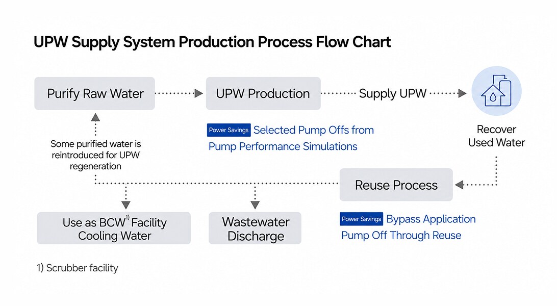
Samsung Semiconductor is reducing Scope 2 emissions by optimizing the operational efficiency of power-intensive equipment and infrastructure. Through this, we are minimizing energy loss by tailoring UPW (Ultra Pure Water) supply to real-time process demand.
Additionally, advanced HVAC control systems have reduced chilled water usage by approximately 70%, significantly lowering the power consumption of pumps and chillers.
Samsung Semiconductor is reducing Scope 2 emissions by optimizing the operational efficiency of power-intensive equipment and infrastructure. Through this, we are minimizing energy loss by tailoring UPW (Ultra Pure Water) supply to real-time process demand.
Additionally, advanced HVAC control systems have reduced chilled water usage by approximately 70%, significantly lowering the power consumption of pumps and chillers.
Samsung Semiconductor is reducing Scope 2 emissions by optimizing the operational efficiency of power-intensive equipment and infrastructure. Through this, we are minimizing energy loss by tailoring UPW (Ultra Pure Water) supply to real-time process demand.
Additionally, advanced HVAC control systems have reduced chilled water usage by approximately 70%, significantly lowering the power consumption of pumps and chillers.
Samsung Semiconductor has been expanding the deployment of smart lighting systems, beginning with selected parking towers in 2024. These systems automatically control illuminance based on natural lighting and the time of day to optimize energy use. By 2025, the company has installed a cumulative total of 17,000 smart lights across all parking towers at the Giheung, Hwaseong, and Pyeongtaek sites.
Samsung Semiconductor has been expanding the deployment of smart lighting systems, beginning with selected parking towers in 2024. These systems automatically control illuminance based on natural lighting and the time of day to optimize energy use. By 2025, the company has installed a cumulative total of 17,000 smart lights across all parking towers at the Giheung, Hwaseong, and Pyeongtaek sites.
Samsung Semiconductor has been expanding the deployment of smart lighting systems, beginning with selected parking towers in 2024. These systems automatically control illuminance based on natural lighting and the time of day to optimize energy use. By 2025, the company has installed a cumulative total of 17,000 smart lights across all parking towers at the Giheung, Hwaseong, and Pyeongtaek sites.
Samsung Semiconductor has been powering all of its overseas business sites with 100% renewable energy since 2020 and is steadily increasing the renewable energy transition rate across its domestic sites.
Samsung Semiconductor has been powering all of its overseas business sites with 100% renewable energy since 2020 and is steadily increasing the renewable energy transition rate across its domestic sites.
Samsung Semiconductor has been powering all of its overseas business sites with 100% renewable energy since 2020 and is steadily increasing the renewable energy transition rate across its domestic sites.
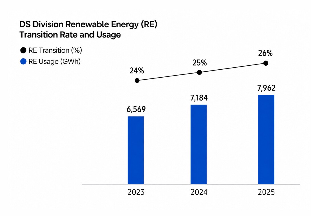
To expand this transition, the company utilizes a diverse range of procurement methods, including Power Purchase Agreements (PPAs), the purchase of Renewable Energy Certificates (RECs), and the implementation of on-site self-generation.
In Korea, Samsung Semiconductor expanded its renewable energy capacity by signing six new PPAs in 2025, totaling 252MW. This brings the cumulative total to 11 PPA contracts with a capacity of 681MW. Additionally, the company has increased its cumulative solar self-generation capacity at domestic and overseas sites to 7.6MW, directly producing and utilizing 5.7GWh of power in 2025 alone.
To expand this transition, the company utilizes a diverse range of procurement methods, including Power Purchase Agreements (PPAs), the purchase of Renewable Energy Certificates (RECs), and the implementation of on-site self-generation.
In Korea, Samsung Semiconductor expanded its renewable energy capacity by signing six new PPAs in 2025, totaling 252MW. This brings the cumulative total to 11 PPA contracts with a capacity of 681MW. Additionally, the company has increased its cumulative solar self-generation capacity at domestic and overseas sites to 7.6MW, directly producing and utilizing 5.7GWh of power in 2025 alone.
To expand this transition, the company utilizes a diverse range of procurement methods, including Power Purchase Agreements (PPAs), the purchase of Renewable Energy Certificates (RECs), and the implementation of on-site self-generation.
In Korea, Samsung Semiconductor expanded its renewable energy capacity by signing six new PPAs in 2025, totaling 252MW. This brings the cumulative total to 11 PPA contracts with a capacity of 681MW. Additionally, the company has increased its cumulative solar self-generation capacity at domestic and overseas sites to 7.6MW, directly producing and utilizing 5.7GWh of power in 2025 alone.
To meet the demands of global Big Tech customers for products supplied via carbon-free energy, Samsung Semiconductor is expanding its use of renewable energy and exploring various carbon reduction strategies utilizing carbon-free energy sources recognized by its customers.
We are also diversifying its reduction methods through academic-industrial collaborations; in 2025, it conducted four research projects on carbon-free energy transition and related policies in partnership with institutions such as Seoul National University and Hanyang University. Furthermore, Samsung Semiconductor actively participates in the board and working groups of the Carbon-Free Energy (CFE) Alliance to contribute to discussions on international technical standards and certification systems for carbon-free energy.
To meet the demands of global Big Tech customers for products supplied via carbon-free energy, Samsung Semiconductor is expanding its use of renewable energy and exploring various carbon reduction strategies utilizing carbon-free energy sources recognized by its customers.
We are also diversifying its reduction methods through academic-industrial collaborations; in 2025, it conducted four research projects on carbon-free energy transition and related policies in partnership with institutions such as Seoul National University and Hanyang University. Furthermore, Samsung Semiconductor actively participates in the board and working groups of the Carbon-Free Energy (CFE) Alliance to contribute to discussions on international technical standards and certification systems for carbon-free energy.
To meet the demands of global Big Tech customers for products supplied via carbon-free energy, Samsung Semiconductor is expanding its use of renewable energy and exploring various carbon reduction strategies utilizing carbon-free energy sources recognized by its customers.
We are also diversifying its reduction methods through academic-industrial collaborations; in 2025, it conducted four research projects on carbon-free energy transition and related policies in partnership with institutions such as Seoul National University and Hanyang University. Furthermore, Samsung Semiconductor actively participates in the board and working groups of the Carbon-Free Energy (CFE) Alliance to contribute to discussions on international technical standards and certification systems for carbon-free energy.
Tech Blog
[SEMICON JAPAN] Samsung Semiconductor Leads Collaborative Carbon Reduction with Alternative Gases
[SEMICON JAPAN] Samsung Semiconductor Leads Collaborative Carbon Reduction with Alternative Gases
[SEMICON JAPAN] Samsung Semiconductor Leads Collaborative Carbon Reduction with Alternative Gases
Tech Blog
[CES Innovation Awards® 2026 Honoree] LPDDR6: World’s First Next-Gen LPDDR Optimized for High-Performing On-Device AI
[CES Innovation Awards® 2026 Honoree] LPDDR6: World’s First Next-Gen LPDDR Optimized for High-Performing On-Device AI
[CES Innovation Awards® 2026 Honoree] LPDDR6: World’s First Next-Gen LPDDR Optimized for High-Performing On-Device AI
Tech Blog
Driving Display Innovation: 22nm Mobile Display Driver IC Makes Low Power the Norm
Driving Display Innovation: 22nm Mobile Display Driver IC Makes Low Power the Norm
Driving Display Innovation: 22nm Mobile Display Driver IC Makes Low Power the Norm
Planet
From raw materials to disposal, efforts to reduce carbon
From raw materials to disposal, efforts to reduce carbon
From raw materials to disposal, efforts to reduce carbon
Planet
Samsung Semiconductor prioritizes the management of suppliers with high emission proportions based on Product Carbon Footprint (PCF) analysis. To ensure accuracy, we calculate and verify emissions through a specialized system integrated with procurement data.
In collaboration with key suppliers, Samsung Semiconductor establishes greenhouse gas reduction targets and regularly monitors their implementation status. As a result, 82% of key suppliers had established reduction targets as of 2025. Furthermore, we provide practical support for tangible reduction activities, such as improving energy efficiency and transitioning to cleaner fuels, through greenhouse gas management training, technical exchange sessions, one-on-one on-site consulting, and the utilization of an ESG fund.
Samsung Semiconductor prioritizes the management of suppliers with high emission proportions based on Product Carbon Footprint (PCF) analysis. To ensure accuracy, we calculate and verify emissions through a specialized system integrated with procurement data.
In collaboration with key suppliers, Samsung Semiconductor establishes greenhouse gas reduction targets and regularly monitors their implementation status. As a result, 82% of key suppliers had established reduction targets as of 2025. Furthermore, we provide practical support for tangible reduction activities, such as improving energy efficiency and transitioning to cleaner fuels, through greenhouse gas management training, technical exchange sessions, one-on-one on-site consulting, and the utilization of an ESG fund.
Samsung Semiconductor prioritizes the management of suppliers with high emission proportions based on Product Carbon Footprint (PCF) analysis. To ensure accuracy, we calculate and verify emissions through a specialized system integrated with procurement data.
In collaboration with key suppliers, Samsung Semiconductor establishes greenhouse gas reduction targets and regularly monitors their implementation status. As a result, 82% of key suppliers had established reduction targets as of 2025. Furthermore, we provide practical support for tangible reduction activities, such as improving energy efficiency and transitioning to cleaner fuels, through greenhouse gas management training, technical exchange sessions, one-on-one on-site consulting, and the utilization of an ESG fund.
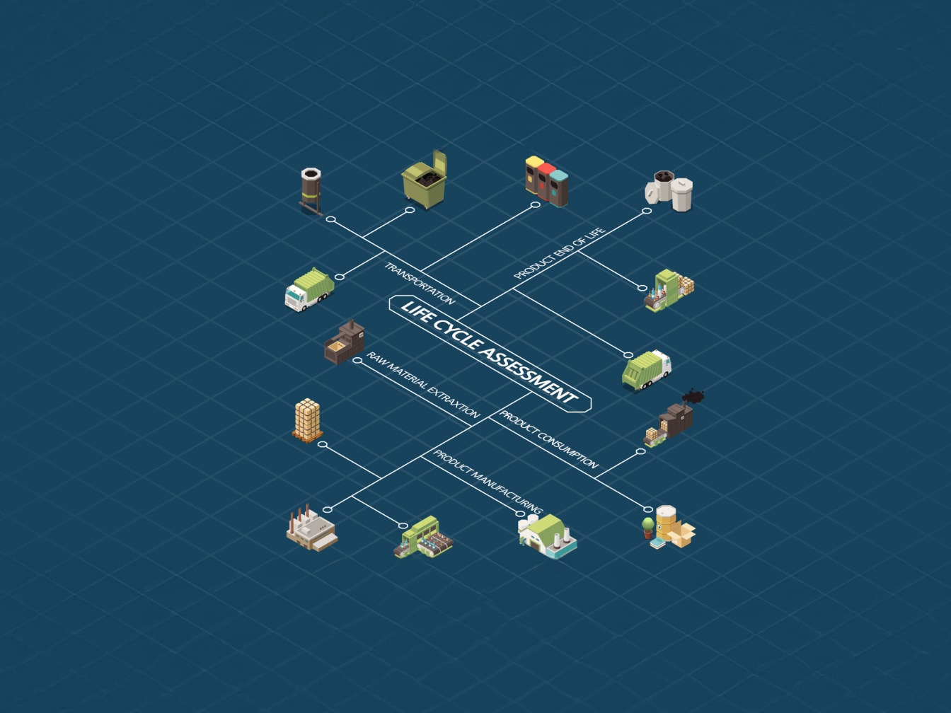
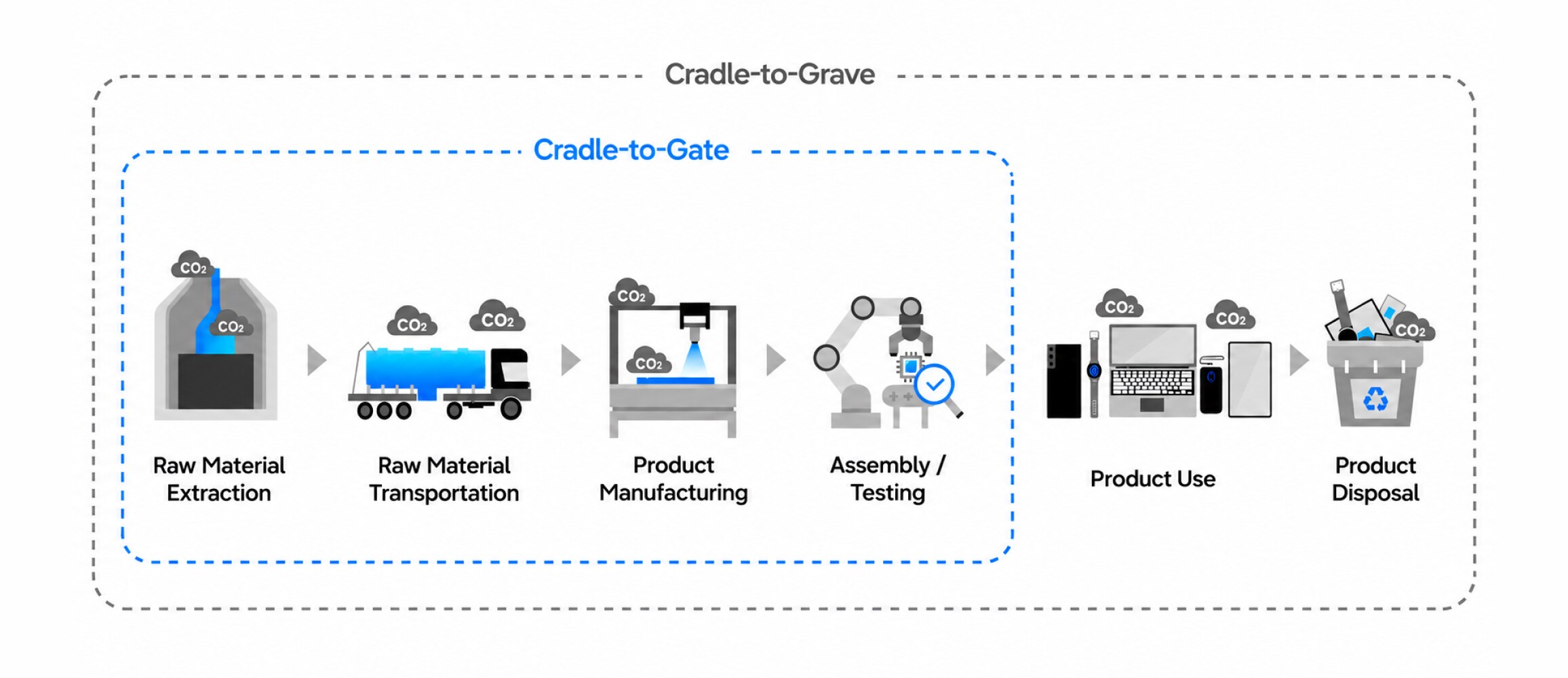
Samsung Semiconductor calculates and manages carbon emissions on a per-product basis, covering the entire lifecycle from raw material extraction to product shipment. Utilizing an automated Product Carbon Footprint (PCF) system based on international standards and Life Cycle Assessment (LCA) processes, we collect detailed activity data, including raw material input, energy consumption, and waste generation. By applying emission factors from the Life Cycle Inventory (LCI) database, we precisely determine the emissions generated throughout the product manufacturing process.
Based on these calculation results, we identify emissions by business site and process to establish targeted reduction measures centered on major emission sources. We ensure the reliability of our findings through regular data updates and rigorous third-party verification. Moving forward, we plan to continuously improve the accuracy of our PCF by supporting suppliers in directly calculating the footprints of raw materials supplied to Samsung Semiconductor and increasing the proportion of primary data integrated into our system.
Samsung Semiconductor calculates and manages carbon emissions on a per-product basis, covering the entire lifecycle from raw material extraction to product shipment. Utilizing an automated Product Carbon Footprint (PCF) system based on international standards and Life Cycle Assessment (LCA) processes, we collect detailed activity data, including raw material input, energy consumption, and waste generation. By applying emission factors from the Life Cycle Inventory (LCI) database, we precisely determine the emissions generated throughout the product manufacturing process.
Based on these calculation results, we identify emissions by business site and process to establish targeted reduction measures centered on major emission sources. We ensure the reliability of our findings through regular data updates and rigorous third-party verification. Moving forward, we plan to continuously improve the accuracy of our PCF by supporting suppliers in directly calculating the footprints of raw materials supplied to Samsung Semiconductor and increasing the proportion of primary data integrated into our system.
Samsung Semiconductor calculates and manages carbon emissions on a per-product basis, covering the entire lifecycle from raw material extraction to product shipment. Utilizing an automated Product Carbon Footprint (PCF) system based on international standards and Life Cycle Assessment (LCA) processes, we collect detailed activity data, including raw material input, energy consumption, and waste generation. By applying emission factors from the Life Cycle Inventory (LCI) database, we precisely determine the emissions generated throughout the product manufacturing process.
Based on these calculation results, we identify emissions by business site and process to establish targeted reduction measures centered on major emission sources. We ensure the reliability of our findings through regular data updates and rigorous third-party verification. Moving forward, we plan to continuously improve the accuracy of our PCF by supporting suppliers in directly calculating the footprints of raw materials supplied to Samsung Semiconductor and increasing the proportion of primary data integrated into our system.
We are improving the energy efficiency of our semiconductor products and manufacturing processes to deliver the same data processing performance with reduced power consumption. As part of these efforts, we are supplying HBM4 and PM1763, both of which offer enhanced power efficiency over previous generations. We have set targets to improve the energy efficiency of HBM and server SSDs by 2.5 times and 4 times, respectively, by 2030 compared to 2025 levels.
Our commitment to efficiency extends to our system LSI and foundry businesses. We are developing high-efficiency products such as the Exynos 2600 and implementing advanced technologies—including EUV1) processes and GAA2) transistor structures—to lower operating voltages and power consumption. Through these innovations, we are helping our customers reduce power consumption and carbon emissions during the use of their AI servers and mobile devices.
We are improving the energy efficiency of our semiconductor products and manufacturing processes to deliver the same data processing performance with reduced power consumption. As part of these efforts, we are supplying HBM4 and PM1763, both of which offer enhanced power efficiency over previous generations. We have set targets to improve the energy efficiency of HBM and server SSDs by 2.5 times and 4 times, respectively, by 2030 compared to 2025 levels.
Our commitment to efficiency extends to our system LSI and foundry businesses. We are developing high-efficiency products such as the Exynos 2600 and implementing advanced technologies—including EUV1) processes and GAA2) transistor structures—to lower operating voltages and power consumption. Through these innovations, we are helping our customers reduce power consumption and carbon emissions during the use of their AI servers and mobile devices.
We are improving the energy efficiency of our semiconductor products and manufacturing processes to deliver the same data processing performance with reduced power consumption. As part of these efforts, we are supplying HBM4 and PM1763, both of which offer enhanced power efficiency over previous generations. We have set targets to improve the energy efficiency of HBM and server SSDs by 2.5 times and 4 times, respectively, by 2030 compared to 2025 levels.
Our commitment to efficiency extends to our system LSI and foundry businesses. We are developing high-efficiency products such as the Exynos 2600 and implementing advanced technologies—including EUV1) processes and GAA2) transistor structures—to lower operating voltages and power consumption. Through these innovations, we are helping our customers reduce power consumption and carbon emissions during the use of their AI servers and mobile devices.
Tech Blog
[SEMICON JAPAN] Samsung Semiconductor Leads Collaborative Carbon Reduction with Alternative Gases
[SEMICON JAPAN] Samsung Semiconductor Leads Collaborative Carbon Reduction with Alternative Gases
[SEMICON JAPAN] Samsung Semiconductor Leads Collaborative Carbon Reduction with Alternative Gases
Tech Blog
[CES Innovation Awards® 2026 Honoree] LPDDR6: World’s First Next-Gen LPDDR Optimized for High-Performing On-Device AI
[CES Innovation Awards® 2026 Honoree] LPDDR6: World’s First Next-Gen LPDDR Optimized for High-Performing On-Device AI
[CES Innovation Awards® 2026 Honoree] LPDDR6: World’s First Next-Gen LPDDR Optimized for High-Performing On-Device AI
Tech Blog
Driving Display Innovation: 22nm Mobile Display Driver IC Makes Low Power the Norm
Driving Display Innovation: 22nm Mobile Display Driver IC Makes Low Power the Norm
Driving Display Innovation: 22nm Mobile Display Driver IC Makes Low Power the Norm
Planet
From raw materials to disposal, efforts to reduce carbon
From raw materials to disposal, efforts to reduce carbon
From raw materials to disposal, efforts to reduce carbon
Planet

 Global