
Samsung Semiconductor is improving its systems and on-site operations with the goal of achieving a 99.9% waste recycling rate by 2030 across its five domestic manufacturing sites.
Recognizing waste not simply as something to be disposed of, but as a valuable resource, we are expanding the range of recyclable items by identifying various recycling technologies and processing partners. It is also broadening the scope of resource circulation by reusing materials and components used in semiconductor manufacturing.
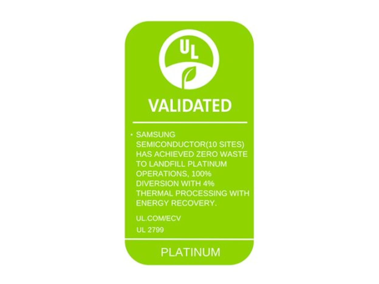
As a result of these efforts, Samsung Semiconductor’s all manufacturing sites have collectively achieved the Platinum grade of Zero Waste to Landfill (ZWTL) certification. We also continue to advance its management indicators in line with evolving regulations and policies related to resource circulation in Korea and overseas.
Samsung Semiconductor is improving its systems and on-site operations with the goal of achieving a 99.9% waste recycling rate by 2030 across its five domestic manufacturing sites.
Recognizing waste not simply as something to be disposed of, but as a valuable resource, we are expanding the range of recyclable items by identifying various recycling technologies and processing partners. It is also broadening the scope of resource circulation by reusing materials and components used in semiconductor manufacturing.
As a result of these efforts, Samsung Semiconductor’s all manufacturing sites have collectively achieved the Platinum grade of Zero Waste to Landfill (ZWTL) certification. We also continue to advance its management indicators in line with evolving regulations and policies related to resource circulation in Korea and overseas.
Samsung Semiconductor is improving its systems and on-site operations with the goal of achieving a 99.9% waste recycling rate by 2030 across its five domestic manufacturing sites.
Recognizing waste not simply as something to be disposed of, but as a valuable resource, we are expanding the range of recyclable items by identifying various recycling technologies and processing partners. It is also broadening the scope of resource circulation by reusing materials and components used in semiconductor manufacturing.
As a result of these efforts, Samsung Semiconductor’s all manufacturing sites have collectively achieved the Platinum grade of Zero Waste to Landfill (ZWTL) certification. We also continue to advance its management indicators in line with evolving regulations and policies related to resource circulation in Korea and overseas.
Samsung Semiconductor has comprehensively improved its waste classification standards and treatment processes to recycle waste that was previously treated through incineration, neutralization, solidification, and other methods.
In particular, by further sorting mixed waste streams by type to identify as many recyclable materials as possible, while securing appropriate recycling partners and applying relevant technologies, Samsung Semiconductor achieved a 99.3% recycling rate at its domestic manufacturing sites in 2025.
Samsung Semiconductor has comprehensively improved its waste classification standards and treatment processes to recycle waste that was previously treated through incineration, neutralization, solidification, and other methods.
In particular, by further sorting mixed waste streams by type to identify as many recyclable materials as possible, while securing appropriate recycling partners and applying relevant technologies, Samsung Semiconductor achieved a 99.3% recycling rate at its domestic manufacturing sites in 2025.
Samsung Semiconductor has comprehensively improved its waste classification standards and treatment processes to recycle waste that was previously treated through incineration, neutralization, solidification, and other methods.
In particular, by further sorting mixed waste streams by type to identify as many recyclable materials as possible, while securing appropriate recycling partners and applying relevant technologies, Samsung Semiconductor achieved a 99.3% recycling rate at its domestic manufacturing sites in 2025.
![[CES Innovation Awards® 2026 Honoree] Portable SSD T7 Resurrected: 100% Recycled Aluminum Body Case and Recyclable Packaging, Designed for Circular Resource Use](https://image.semiconductor.samsung.com/image/samsung/p6/semiconductor/newsroom/t7-resurrected/article-t7-4x3.png?$ORIGIN_PNG$)
Tech Blog
Samsung Semiconductor Newsroom
Samsung Electronics Achieves UL Solutions’ ‘Zero Waste to Landfill’ Platinum Designation Across All Global Manufacturing Sites
Samsung Electronics Achieves UL Solutions’ ‘Zero Waste to Landfill’ Platinum Designation Across All Global Manufacturing Sites
Samsung Electronics Achieves UL Solutions’ ‘Zero Waste to Landfill’ Platinum Designation Across All Global Manufacturing Sites
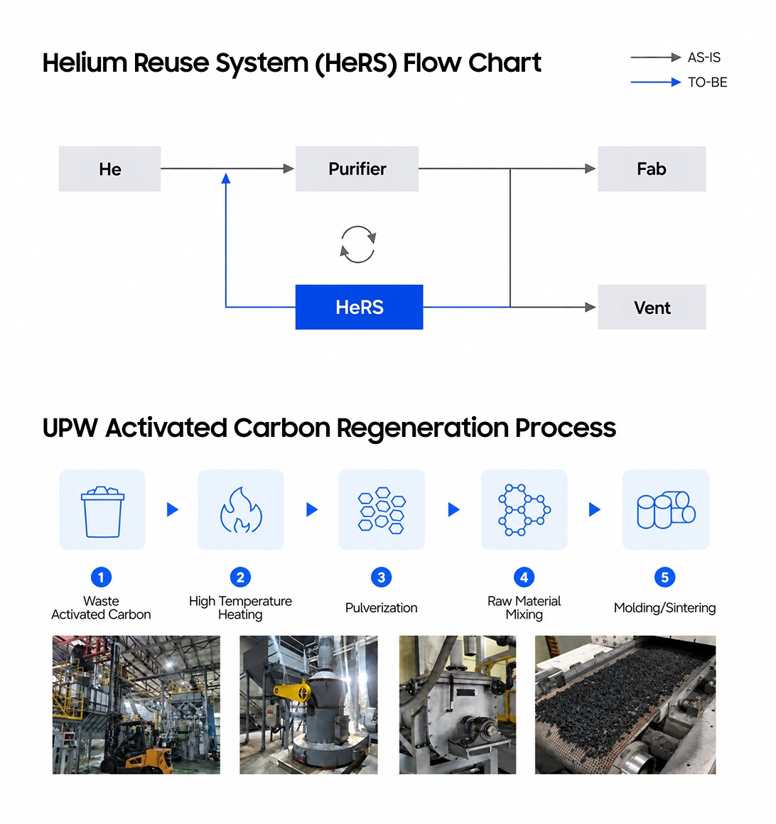
Samsung Semiconductor is applying regeneration technologies to materials used in semiconductor processes, partially replacing new material purchases and helping secure a more stable material supply.
In particular, we developed the industry’s first system for reusing helium, one of the key materials used in semiconductor manufacturing. It is also working to expand the application of regeneration technologies to other major process materials with potential supply chain risks.
In addition, Samsung Semiconductor identified a partner with technology to regenerate activated carbon used in wastewater treatment and low-concentration odor removal. As a result, approximately 90% of activated carbon that was previously incinerated has been converted to recycling.
Samsung Semiconductor is applying regeneration technologies to materials used in semiconductor processes, partially replacing new material purchases and helping secure a more stable material supply.
In particular, we developed the industry’s first system for reusing helium, one of the key materials used in semiconductor manufacturing. It is also working to expand the application of regeneration technologies to other major process materials with potential supply chain risks.
In addition, Samsung Semiconductor identified a partner with technology to regenerate activated carbon used in wastewater treatment and low-concentration odor removal. As a result, approximately 90% of activated carbon that was previously incinerated has been converted to recycling.
Samsung Semiconductor is applying regeneration technologies to materials used in semiconductor processes, partially replacing new material purchases and helping secure a more stable material supply.
In particular, we developed the industry’s first system for reusing helium, one of the key materials used in semiconductor manufacturing. It is also working to expand the application of regeneration technologies to other major process materials with potential supply chain risks.
In addition, Samsung Semiconductor identified a partner with technology to regenerate activated carbon used in wastewater treatment and low-concentration odor removal. As a result, approximately 90% of activated carbon that was previously incinerated has been converted to recycling.
Tech Blog
Samsung Semiconductor Newsroom
Samsung Electronics Achieves UL Solutions’ ‘Zero Waste to Landfill’ Platinum Designation Across All Global Manufacturing Sites
Samsung Electronics Achieves UL Solutions’ ‘Zero Waste to Landfill’ Platinum Designation Across All Global Manufacturing Sites
Samsung Electronics Achieves UL Solutions’ ‘Zero Waste to Landfill’ Platinum Designation Across All Global Manufacturing Sites
Samsung Semiconductor has been strengthening resource circulation beyond individual business divisions. In collaboration with the Circular Economy Research Lab of the DX Division, waste wafer trays generated during semiconductor production have been reprocessed into recycled plastic and applied to components of the Galaxy S25 series.1)
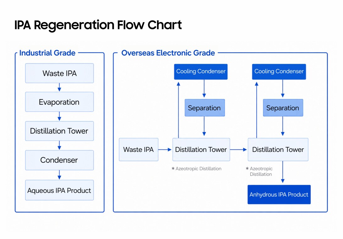
We are also increasing the value of waste resources by recycling waste IPA2) generated after use in semiconductor cleaning processes. Through a high-purity purification process, the waste IPA is recycled into industrial-grade IPA and overseas electronic-grade IPA3).
Samsung Semiconductor has been strengthening resource circulation beyond individual business divisions. In collaboration with the Circular Economy Research Lab of the DX Division, waste wafer trays generated during semiconductor production have been reprocessed into recycled plastic and applied to components of the Galaxy S25 series.1)
We are also increasing the value of waste resources by recycling waste IPA2) generated after use in semiconductor cleaning processes. Through a high-purity purification process, the waste IPA is recycled into industrial-grade IPA and overseas electronic-grade IPA3).
Samsung Semiconductor has been strengthening resource circulation beyond individual business divisions. In collaboration with the Circular Economy Research Lab of the DX Division, waste wafer trays generated during semiconductor production have been reprocessed into recycled plastic and applied to components of the Galaxy S25 series.1)
We are also increasing the value of waste resources by recycling waste IPA2) generated after use in semiconductor cleaning processes. Through a high-purity purification process, the waste IPA is recycled into industrial-grade IPA and overseas electronic-grade IPA3).
Tech Blog
Samsung Semiconductor Newsroom
Samsung Electronics Achieves UL Solutions’ ‘Zero Waste to Landfill’ Platinum Designation Across All Global Manufacturing Sites
Samsung Electronics Achieves UL Solutions’ ‘Zero Waste to Landfill’ Platinum Designation Across All Global Manufacturing Sites
Samsung Electronics Achieves UL Solutions’ ‘Zero Waste to Landfill’ Platinum Designation Across All Global Manufacturing Sites
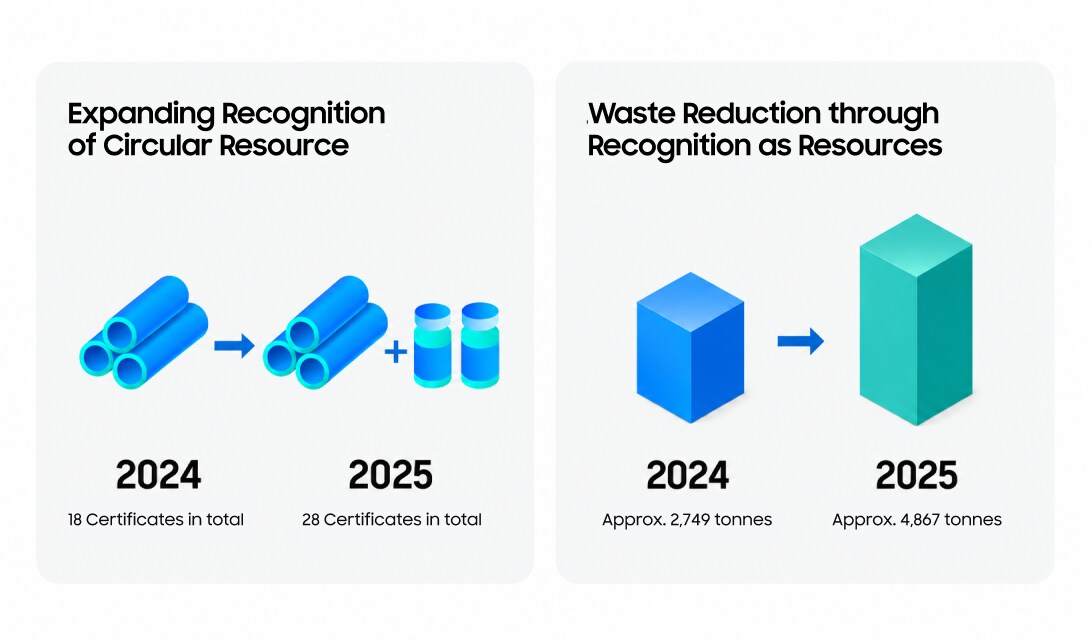
The Circular Resource Recognition System recognizes waste that meets the standards under the Act on Promotion of Transition to Circular Economy and Society1), introduced in 2018, as 'resources' that can be used again.
Samsung Semiconductor has continued to obtain Circular Resource Recognition certifications since 2019. As of 2025, we have secured a cumulative total of 28 certifications across our worksites, converting approximately 4,867 tons of waste into resources.
The Circular Resource Recognition System recognizes waste that meets the standards under the Act on Promotion of Transition to Circular Economy and Society1), introduced in 2018, as 'resources' that can be used again.
Samsung Semiconductor has continued to obtain Circular Resource Recognition certifications since 2019. As of 2025, we have secured a cumulative total of 28 certifications across our worksites, converting approximately 4,867 tons of waste into resources.
The Circular Resource Recognition System recognizes waste that meets the standards under the Act on Promotion of Transition to Circular Economy and Society1), introduced in 2018, as 'resources' that can be used again.
Samsung Semiconductor has continued to obtain Circular Resource Recognition certifications since 2019. As of 2025, we have secured a cumulative total of 28 certifications across our worksites, converting approximately 4,867 tons of waste into resources.
Tech Blog
Samsung Semiconductor Newsroom
Samsung Electronics Achieves UL Solutions’ ‘Zero Waste to Landfill’ Platinum Designation Across All Global Manufacturing Sites
Samsung Electronics Achieves UL Solutions’ ‘Zero Waste to Landfill’ Platinum Designation Across All Global Manufacturing Sites
Samsung Electronics Achieves UL Solutions’ ‘Zero Waste to Landfill’ Platinum Designation Across All Global Manufacturing Sites
Samsung Semiconductor continuously monitors packaging-related regulatory trends in key markets, while expanding the use of recycled materials and reducing packaging across its products and packaging.
Samsung Semiconductor continuously monitors packaging-related regulatory trends in key markets, while expanding the use of recycled materials and reducing packaging across its products and packaging.
Samsung Semiconductor continuously monitors packaging-related regulatory trends in key markets, while expanding the use of recycled materials and reducing packaging across its products and packaging.
In 2024, Samsung Semiconductor recycled waste aluminum and applied it to the case of the Portable SSD T7 Shield. In 2025, the application was expanded to the case of the Portable SSD T7 Resurrected.
In 2024, Samsung Semiconductor recycled waste aluminum and applied it to the case of the Portable SSD T7 Shield. In 2025, the application was expanded to the case of the Portable SSD T7 Resurrected.
In 2024, Samsung Semiconductor recycled waste aluminum and applied it to the case of the Portable SSD T7 Shield. In 2025, the application was expanded to the case of the Portable SSD T7 Resurrected.

To reduce plastic packaging, Samsung Semiconductor is gradually transitioning SSD packaging trays to paper-based materials. Starting with consumer SSDs in 2020, we completed the transition for Portable SSD and Heatsink products in 2023, and 2.5-inch products in 2024. In 2026, it plans to expand the application to M.2 products.
To reduce plastic packaging, Samsung Semiconductor is gradually transitioning SSD packaging trays to paper-based materials. Starting with consumer SSDs in 2020, we completed the transition for Portable SSD and Heatsink products in 2023, and 2.5-inch products in 2024. In 2026, it plans to expand the application to M.2 products.
To reduce plastic packaging, Samsung Semiconductor is gradually transitioning SSD packaging trays to paper-based materials. Starting with consumer SSDs in 2020, we completed the transition for Portable SSD and Heatsink products in 2023, and 2.5-inch products in 2024. In 2026, it plans to expand the application to M.2 products.
Tech Blog
Samsung Semiconductor Newsroom
Samsung Electronics Achieves UL Solutions’ ‘Zero Waste to Landfill’ Platinum Designation Across All Global Manufacturing Sites
Samsung Electronics Achieves UL Solutions’ ‘Zero Waste to Landfill’ Platinum Designation Across All Global Manufacturing Sites
Samsung Electronics Achieves UL Solutions’ ‘Zero Waste to Landfill’ Platinum Designation Across All Global Manufacturing Sites

 Global