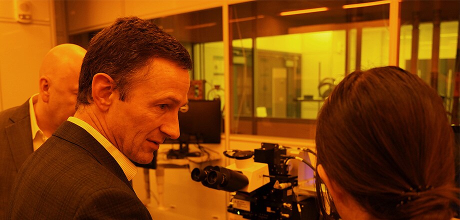
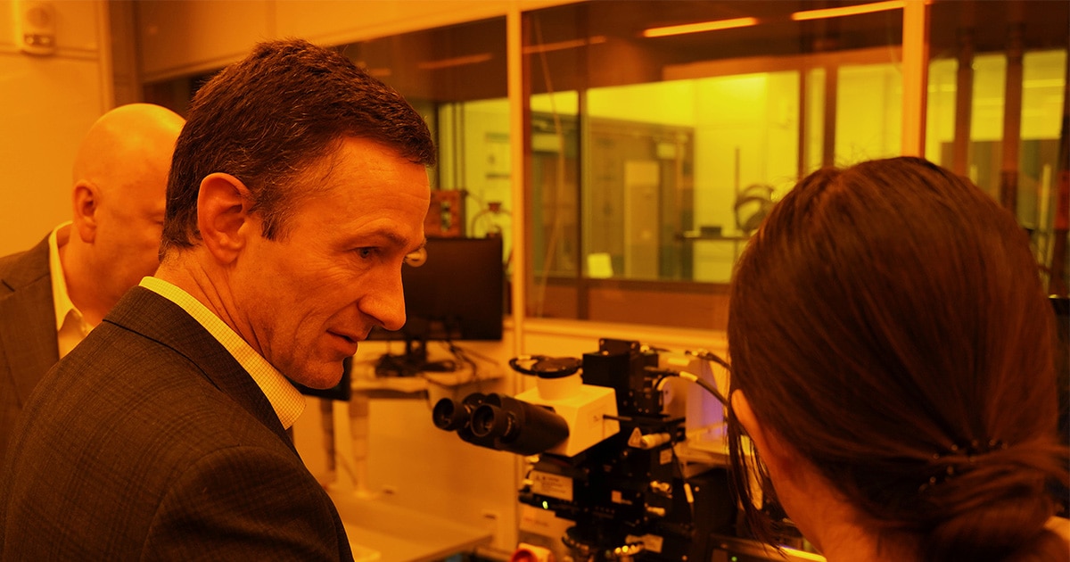
In 2025, The University of Texas at Austin launched a Master's of Semiconductor Science and Engineering (MSSE) program↗ as a way to provide students a deep understanding of the science of semiconductors and how to engineer and manufacture devices and systems around these core disciplines. In a growing industry, the program helps develop the talent pipeline needed for the advanced semiconductor manufacturing sector.
In partnership with UT Austin, Samsung Austin Semiconductor invests in the MSSE program by providing four students $70,000 scholarships that fully cover the cost of the program. They are also usually given the opportunity to intern with us during the summer while they work on their masters’ research project.
For the 2025-2026 school year, six projects are underway with direct management from Samsung Semiconductor researchers, including Shyan Byrapa (two projects), Haewon Kim (two projects), Eric Bruce (one project) and Yan Li (one project). According to the university, current enrollment stands at 24 students, with plans to recruit an additional 24 students for Fall 2026.
This summer, four graduate students are interning with Samsung Austin Semiconductor. We spoke to two of the students, Eric Chen and Pavan Bharadwaj, about their projects and how their internship with us is enhancing their knowledge of the semiconductor industry.
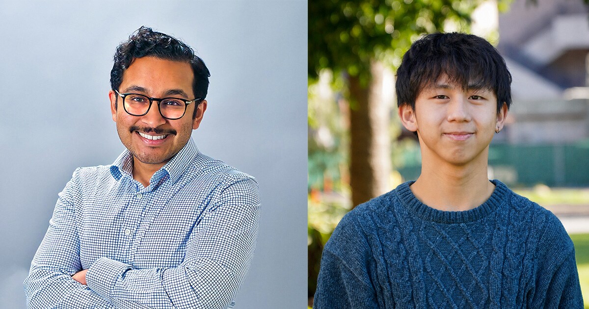
Chen and Bharadwaj are both interning with the Metrology department. Chen has a BS in Chemical Engineering from UC Santa Barbara and Bharadwaj has a BS in Electrical Engineering from Georgia Institute of Technology.
Q: Why did you enroll in UT’s MSSE program?
Bharadwaj: After working in the industry in Dallas, I knew I wanted to stay in Texas and build my career in semiconductors. Around the same time, UT launched its new 3-semester MSSE program, which turned out to be a great fit.
Chen: After my first internship in the industry during college, I wanted to learn more about semiconductors in a structured curriculum with some dedicated hands-on experiences. UT's MSSE was (maybe still is) the only program in the US that offered this learning experience with all expenses covered.
Q: What is your project?
Bharadwaj: Professor Dr. Fangzou Xia has done a wonderful job integrating our cohort into the lab and providing meaningful research opportunities. Given my background in process engineering and interest in process development, my main project is fabricating piezoelectric atomic force microscopy (AFM) cantilevers using aluminum nitride (AlN) as the active layer on SiO2/Si wafers. This involves running and developing a full process flow: pulsed DC reactive sputtering of AlN, X-ray diffraction (XRD) characterization to confirm film stress, piezoresponse force microscopy characterization to verify piezoelectric response, metal deposition of Chromium and Aluminum for the cantilever's metal lines, wet oxidation and deep silicon etches to release the cantilevers from the wafer. Once the fabrication is complete, I will also characterize the cantilevers using our lab's commercial-grade AFM.
In parallel, I'm building a database to help fine-tune AFM parameters by feature type, since probing a trench requires very different settings than probing a Longhorn logo, with the goal of generalizing parameters across commonly probed features.
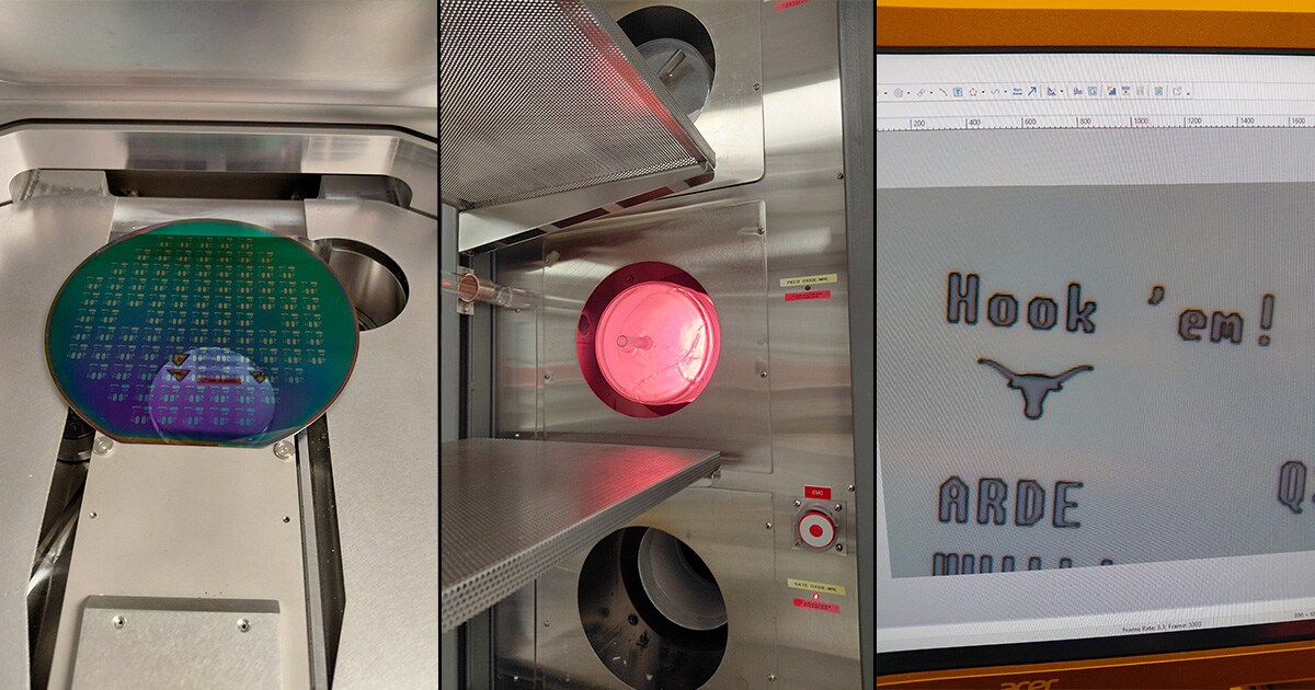
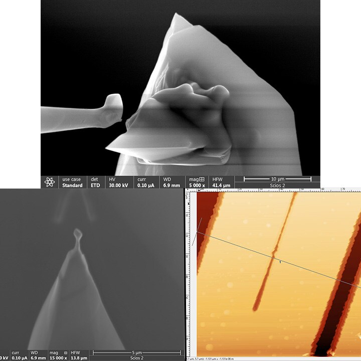
Chen: My project is on developing AFM methods for semiconductor metrology, particularly for imaging deep trenches, sidewalls and buried features. The work combines commercial and custom probes, including focus ion beam-modified tips, with techniques such as contact resonance, torsional resonance and scanning microwave microcopy to resolve imaging challenges for complex devices and defect detections. The project also includes external control and automation development using Python, LabVIEW, FPGA, in conjunction with commercial AFM hardware. The long-term goal for this project is to enable faster and more reliable inline inspection of complex semiconductor structures.
Q: What excites you about your project and Samsung Austin Semiconductor's role in assisting with the project?
Bharadwaj: In my earlier roles as a process and product engineer, I often felt I was missing part of the larger story behind a how a chip comes together. Running my own process end-to-end, from sputtering and hard mask development to etch troubleshooting and XRD analysis, has given me instincts I didn't have before. Because this project spans deposition, lithography, etch and characterization, it's given me a strong appreciation for how changes in one process module ripple downstream.
For my database project, Samsung Austin Semiconductor’s guidance on how their AFM usage has evolved and the challenges they encounter has directly shaped my database project.
Chen: What excites me the most about this project is the concept that I am solving a tangible, ongoing engineering issue in the industry with my knowledge and skillsets. With the involvement of Samsung Austin Semiconductor in the project, not only did I understand how this issue impacts the "real-world" but got to see those issues firsthand by working here. Knowing what problems my work would be able to solve propels me more than anything else.
Q: What has been challenging about the project?
Bharadwaj: I faced a steep learning curve across nearly every process area, and this was compressed into just a few months. Mask alignment, bake temperatures, etch selectivity, hard mask requirements and unfortunately every other step all came with a learning curve that I hadn't appreciated beforehand. Some of my most valuable lessons came from process failures, such as discovering that excessive reactive ion etching power can carbonize photoresist beyond recovery. Working through issues like that has taught me as much about process control as any coursework.
Chen: Coming from a chemical engineering background, the biggest challenge for me were the knowledge gaps I had in the mechanical engineering field. I had to spend a couple of months just reading and filling in the gaps before I actually work on the project. Nevertheless, this allowed me to acquire a whole different set of skills that are definitely worth the while.
Q: In addition to being a part of the MSSE program, you're an intern with us this summer. How is it going?
Bharadwaj: It's been a great experience with the team. Learning how metrology engineers approach risk analysis on a daily basis: rigorous, data-driven and always mindful of downstream impact. That is something that will stick with me for the rest of my career. Also, learning the art of building an optical critical dimension model has been especially eye-opening. I was familiar with ellipsometry in principle, but the depth of analysis required to understand periodicity continues to impress me. Watching the team create models and seeing their intuitive sense for the right adjustments has been a highlight of the summer.
Chen: I really enjoyed the internship experience here. The program is well-structured and I was given access to a variety of very interesting projects and materials. Being able to learn how metrology works in a state-of-the-art semiconductor fab was definitely eye-opening. The best thing is that my team is absolutely fantastic. Everyone responded to my infinite curiosity with kindness and patience. I never once felt unwelcomed when I asked a question, and this applies to everyone I've met here!
Q: What aspects of advanced semiconductor manufacturing were you excited to learn more about during your internship?
Bharadwaj: My prior experience in industry and school was primarily with planar transistors, so I've spent considerable time studying FinFET process flows and scaling challenges. Learning about the engineering problems that had to be solved along the way has been one of the most exciting parts of the internship.
Chen: Having learnt the basic knowledge for semiconductor devices/manufacturing in school, I was most excited to learn more about how a works so efficiently. One of my favorite projects here was the optical critical dimension site reduction project, where we reduced measurement sites while maintaining measurement accuracy/coverage and ended up about 40% more efficient. I really enjoyed learning how each department work in conjunction and what engineering techniques are in place so that the fab can maximize efficiency.
Samsung Austin Semiconductor’s partnership with UT Austin
Supporting the MSSE program is one of the ways Samsung Austin Semiconductor is working to address the workforce needs of the semiconductor industry. Since 2023, Samsung Electronics has invested more than $6 million in workforce and research programs focused on funding student scholarships, fellowships, labs and more.
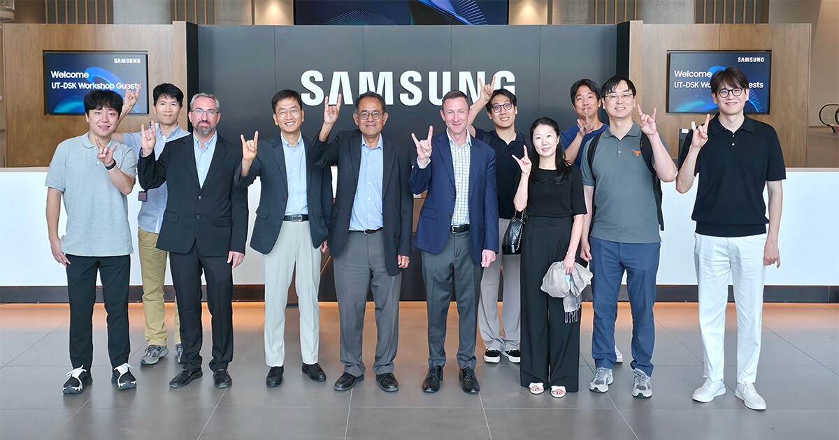
In July, Samsung Austin Semiconductor welcomed three distinguished professors from the MSSE program to our Taylor campus for a workshop hosted by Samsung Semiconductor. During the workshop, the professors shared insights and provided in-depth perspectives on their research projects.

 Global