As AI becomes capable of understanding long documents, answering complex questions, and performing multiple tasks, the demands on the semiconductors behind these capabilities are also increasing. Beyond the compute performance required to train large models, AI systems must respond quickly to user requests while operating efficiently within limited power budgets.
This shift is also driving the evolution of memory. Even the most powerful processor cannot fully utilize its compute resources if data does not arrive fast enough. Storing and delivering more data while reducing the energy required to move it has therefore become a critical challenge for AI systems.
This series explores the role of HBM in AI systems, how the technology is evolving, and Samsung’s next-generation memory solutions. Part 1 looks at why HBM emerged and how it has developed. Part 2 introduces zHBM and the integrated technology capabilities supporting its development.
AI chips are semiconductors designed or used to efficiently perform AI training and inference. GPUs and AI-specific ASICs are key examples, while CPUs typically handle data preprocessing, workload scheduling, and system management.
GPUs became widely used in AI because their highly parallel architecture, originally developed to process large numbers of pixels simultaneously, is also well suited to the matrix operations at the core of deep learning.
GPU efficiency, however, varies by workload. Training workloads with large batches can make extensive use of parallel compute resources, while some inference workloads generate tokens sequentially and may not fully utilize them. During decode at smaller batch sizes, memory bandwidth can become a key performance constraint.
AI-specific ASICs address these requirements by optimizing hardware for targeted workloads. Their focus is on improving performance and power efficiency for specific operations, although actual gains depend on the model and system architecture.
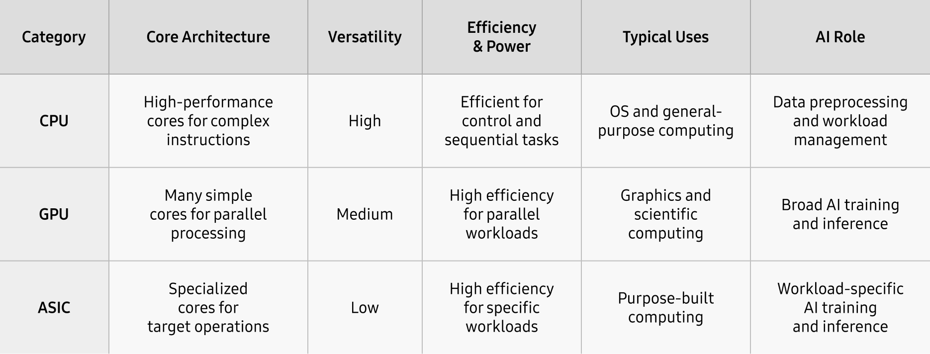
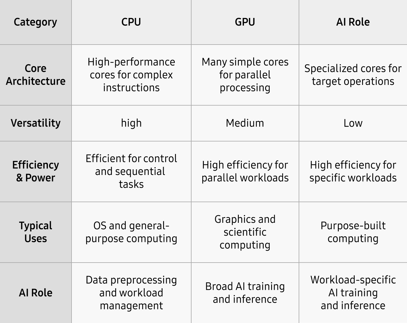
AI GPUs are also evolving with more specialized matrix-compute units and support for multiple numerical precision formats. At the same time, performance optimization is expanding beyond individual chips toward rack-scale architectures that integrate GPUs, CPUs, memory, high-speed interconnects, power delivery, cooling, and software.
To fully utilize accelerator compute resources, data must be available when needed. This is why memory is becoming increasingly important as AI systems evolve.
AI computation requires model weights and data generated during execution. If memory cannot supply data fast enough relative to processor performance, compute resources spend more time waiting than calculating. This imbalance is commonly described as the memory wall.
The same challenge appears in large language model inference. The prefill stage, which processes input tokens, and the decode stage, which generates tokens sequentially, have different computational characteristics. During decode, particularly at smaller batch sizes, the rate at which model weights and KV cache data can be accessed may significantly affect response time.
The KV cache stores keys and values calculated from previous tokens so they can be reused when generating subsequent tokens. As context lengths grow and concurrent requests increase, the amount of data that must be stored and supplied also rises.
Two memory characteristics are especially important: bandwidth and capacity. Bandwidth is the amount of data that can be transferred over time, while capacity is the amount that can be stored.
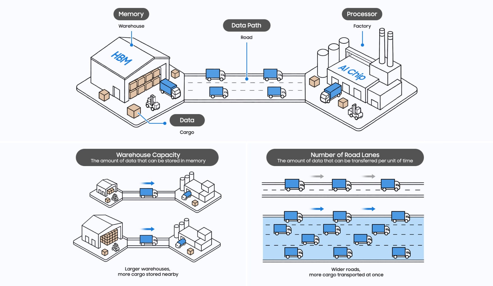
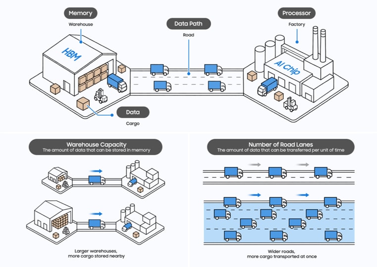
Think of the processor as a factory and memory as a nearby warehouse. Bandwidth is the carrying capacity of the road between them: more lanes allow more goods to move at once. Capacity is the size of the warehouse: more storage keeps more materials close to the factory and reduces the need to retrieve them from farther away.
AI systems face the same challenge. They need enough nearby memory to hold working data and enough bandwidth to deliver it efficiently to the processor.
GPUs have traditionally used GDDR to provide high memory bandwidth. Designed for higher per-pin data rates than conventional DDR, GDDR was well suited to early GPU-based AI workloads.
As AI models grew larger, however, systems needed to scale both bandwidth and capacity. Because GDDR devices are placed around the GPU on the board, adding memory requires additional space and routing. Raising per-pin data rates also increases the challenges of power consumption, heat, and signal integrity.
GDDR continues to advance, but meeting growing data requirements within tight power and space constraints calls for a different approach.
HBM addresses this challenge by combining vertical stacking with a wide I/O interface. Multiple DRAM dies are stacked and connected through Through Silicon Vias (TSVs), enabling large amounts of data to move in parallel.
1. High bandwidth through wide I/O
HBM increases bandwidth not only through higher data rates, but also through a large number of parallel I/O connections. This enables high aggregate bandwidth at lower per-pin data rates than GDDR.
2. Higher capacity through vertical stacking
Stacking DRAM dies vertically provides greater capacity within a limited footprint. Keeping more model weights and KV cache data close to the accelerator can reduce access to slower memory tiers and the resulting latency.
3. Greater energy efficiency through shorter connections
HBM is placed close to the AI chip using technologies such as interposers. Shorter data paths help reduce signal loss and the energy required for data transfer. Combined with a wide parallel interface, this enables high bandwidth without relying solely on very high per-pin speeds.
4. High-density packaging in a smaller footprint
Vertical stacking reduces the area required compared with placing multiple memory devices side by side. Combined with interposer-based 2.5D packaging, multiple HBM stacks can be positioned close to an AI chip within a single package, enabling dense I/O connectivity in limited space.
HBM therefore addresses bandwidth, capacity, power efficiency, and space efficiency together. These characteristics have made it a key memory technology for high-performance AI chips, including GPUs and AI-specific ASICs.
With each generation, HBM has increased bandwidth and capacity, enabling larger models and longer contexts. At the same time, the volume of data that must be stored and moved has continued to grow.
The expansion of inference and reasoning workloads further increases the need to access model weights and KV cache data. As AI requirements evolve, memory bottlenecks can reappear even as memory performance improves.
HBM is therefore advancing through both new generations and continued optimization of existing ones. Bandwidth can be increased through more internal data paths, while capacity can be expanded through higher stack counts—from 8-high to 12-high and 16-high—and higher-density DRAM dies.
Advanced DRAM processes and base dies built on advanced logic technologies also provide new opportunities to improve power efficiency.
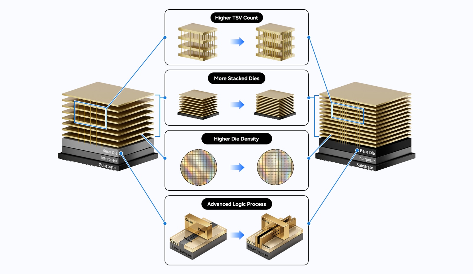
One way to improve data-movement efficiency is to reduce the distance between memory and compute. Shorter connections can deliver more data while reducing the energy required to move it.
Samsung zHBM, currently under development, takes this approach further. Instead of placing memory beside a GPU or AI-specific ASIC, zHBM directly stacks memory on top of the compute device.
By combining direct 3D integration with dense parallel interconnects, zHBM is designed to shorten data paths and increase connectivity between memory and compute. Its architecture also incorporates the thermal considerations introduced by direct stacking, approaching data movement as a system-level optimization challenge.
Part 2 examines how zHBM uses high-density vertical interconnects, lower data-movement energy, and thermal-management technologies to address next-generation AI requirements. It also explores how Samsung’s integrated technology capabilities support co-design and collaboration with customers and partners.

 Global
