Samsung Electronics participated in NVIDIA AI Day Seoul 2026, sharing its latest research in AI-driven semiconductor engineering and highlighting its collaboration with NVIDIA. The event brought together companies and AI ecosystem partners in Korea to share AI technologies and industry use cases.
Samsung’s Computational Science & Engineering (CSE) team from the Semiconductor R&D Center joined NVIDIA for a session titled “Building Autonomous AI Engineers With NVIDIA PhysicsNeMo.” NVIDIA presented its vision and technologies for accelerating semiconductor engineering with AI physics, while Samsung shared its work applying Scientific Machine Learning (SciML) to large-scale semiconductor simulation, along with results from its joint research with NVIDIA.
Semiconductor engineering relies on complex simulations across chip design, manufacturing, packaging, and system-level integration. As semiconductor designs and process technologies become more complex, engineers must account for more variables and run larger, more frequent simulations to identify optimal design and process conditions.
At the session, NVIDIA introduced an AI physics approach that uses simulation data and governing equations to build and train AI models for engineering workflows. The approach can accelerate semiconductor engineering tasks ranging from reducing design turnaround time and optimizing process conditions to accelerating thermal and mechanical analysis. Key technologies include NVIDIA PhysicsNeMo↗, which supports the development of AI physics models, and NVIDIA Warp↗, a Python framework for GPU-accelerated simulation.
Building on this AI physics work, Samsung's collaboration with NVIDIA also extends to GPU acceleration for process, device, and optical simulation, as well as materials research. In TCAD, joint work focuses on NVIDIA cuISS↗ and NVIDIA cuDSS↗ for sparse linear systems. In materials research, NVIDIA cuEST↗ is being integrated into Samsung’s molecular DFT platform, sMOL, to accelerate electronic-structure calculations, while work with NVIDIA cuEquivariance↗ explores faster training and inference for atomistic AI models.
To connect simulation tools and AI physics models within engineering workflows, NVIDIA also introduced an agent-based approach. With the NVIDIA Agent Toolkit↗, an agent can translate a design objective into simulation inputs such as geometry, materials, and boundary conditions, invoke AI predictions or high-fidelity numerical solvers as needed, evaluate the results, and select the next design candidates to explore. The agent orchestrates tools and execution environments, while AI physics models and numerical solvers perform the underlying physics calculations.
NVIDIA Agent Toolkit for design and engineering
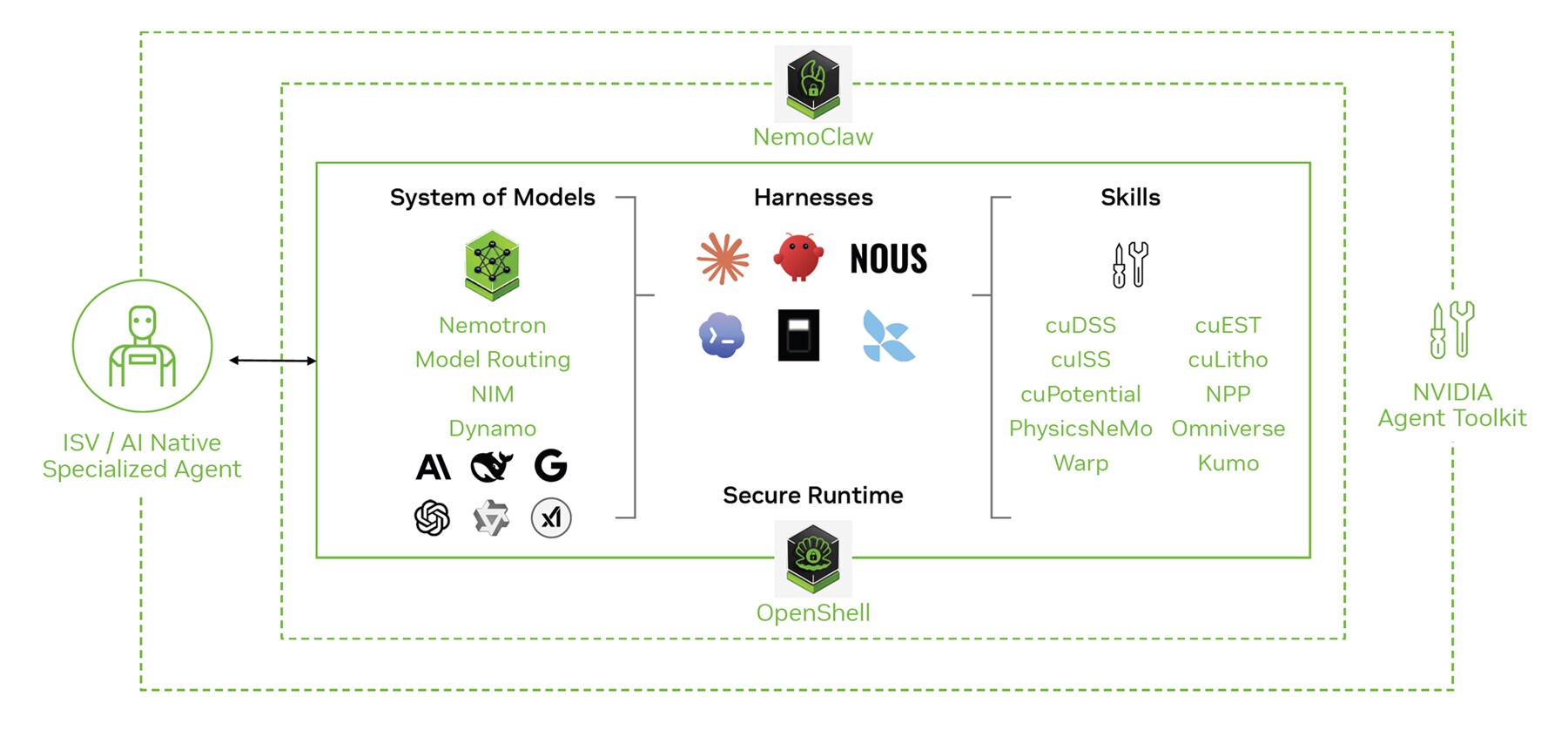
One area where this broader AI physics approach can make a tangible difference is chip-scale thermal and mechanical simulation, a challenge Samsung’s CSE team has been working to address.
Reliable product design depends on accurately predicting thermal behavior, stress, and deformation across complex structures. However, resolving those structures in fine detail can quickly drive up computational cost and simulation time.
To tackle this, Samsung’s CSE team has been advancing SciML, combining physics-based simulation with AI to make these simulations more efficient and scalable.
A key question behind the work is simple:
“Instead of solving the entire problem at once, can we break it into smaller problems, solve them, and then connect the solutions?”
One approach is Domain Decomposition. A large simulation domain is divided into smaller subdomains, with information exchanged across their boundaries until they converge on a consistent overall solution. Samsung’s CSE team developed a foundation-model-based approach that incorporates physical constraints to predict the response of each subdomain while maintaining consistency across the full domain.
The other is Homogenization. Rather than explicitly resolving every detail of a complex microstructure, the team uses AI to predict effective material properties that represent its thermal and mechanical characteristics. These properties can then be used in larger-scale simulations, reducing computational cost while preserving the effects of the underlying microstructure.
Through this work, Samsung’s CSE team has expanded its SciML research from individual problems to methods that can scale to chip-level multi-physics simulations. Related research was published at DAC 2026, and Samsung’s FP-DDM work is also available as a PhysicsNeMo example↗.
The joint session also highlighted how Samsung and NVIDIA are working together to bring these approaches into practical semiconductor engineering.
End-to-end SciML pipeline
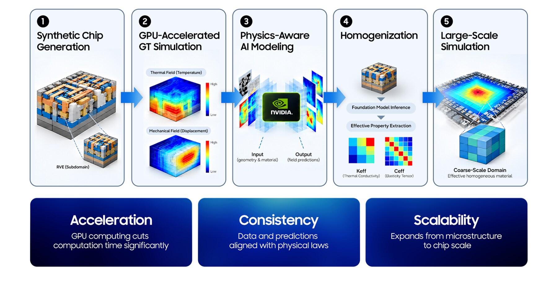
The companies have built an end-to-end SciML pipeline that combines Samsung’s semiconductor simulation expertise with NVIDIA GPU computing and AI physics technologies. The workflow begins by generating synthetic layouts that reflect semiconductor geometry and material properties. A GPU-accelerated solver built with NVIDIA Warp is then used to generate simulation data, which is used to train physics-aware AI models with PhysicsNeMo. The trained models predict effective material properties from complex structures and feed them into larger-scale simulations.
One of the key results is an AI Homogenization workflow for thermal and mechanical simulation. A complex structure represented by roughly 1 billion fine voxels can be represented at a coarser scale with approximately 1 million cells. A simulation that took about 18 hours on a 32-core CPU using a fine-grid solve was completed in just 41 seconds on a single NVIDIA Hopper GPU, using an AI-homogenized coarse-grid solve.
Compared with the fine-grid CPU baseline, the combined AI homogenization and GPU-accelerated workflow delivers an approximately 1,600× speedup, while maintaining 99.17% accuracy in effective vertical thermal conductivity.
By combining semiconductor domain expertise with GPU-accelerated computing and AI models, Samsung and NVIDIA are developing simulation workflows that can improve speed while maintaining physical consistency and scaling to larger and more complex engineering problems.
These results demonstrate how AI physics can accelerate a key step in semiconductor simulation, helping engineers evaluate design options faster. As simulation moves from something engineers have to wait for to something they can interact with in near real time, semiconductor engineering can become more responsive and iterative.
Samsung will continue expanding the use of AI physics and SciML through its collaboration with NVIDIA, exploring how these technologies can ultimately enable Autonomous AI Engineers capable of carrying out increasingly complex engineering tasks.

 Global
