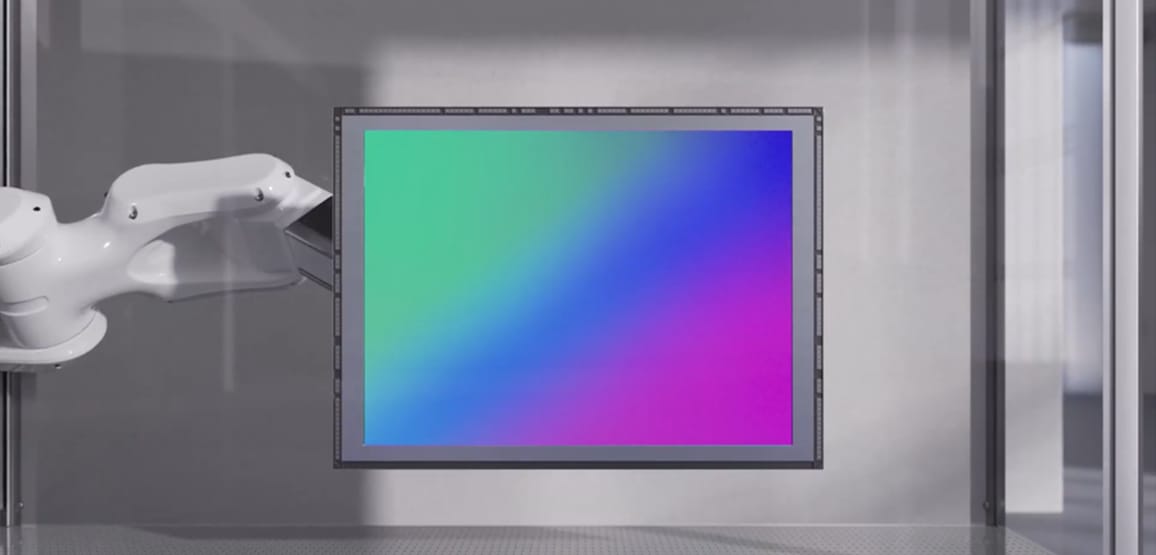
Ultra-fine pixel technology
Ultra-fine pixel technology
Ultra-fine pixel technology
Inspired by ISOCELL
Inspired by ISOCELL
Inspired by ISOCELL
To improve light absorption while shrinking pixels, Samsung’s image sensors have progressed from front side illumination (FSI) to back-side illumination (BSI), which places the photodiode closer to the microlens. Then came ISOCELL technology, which isolates pixels by forming a barrier between them. A key advancement of ISOCELL was the evolution of Back-side Deep Trench Isolation (BDTI) to Front Deep Trench Isolation (FDTI).
To improve light absorption while shrinking pixels, Samsung’s image sensors have progressed from front side illumination (FSI) to back-side illumination (BSI), which places the photodiode closer to the microlens. Then came ISOCELL technology, which isolates pixels by forming a barrier between them. A key advancement of ISOCELL was the evolution of Back-side Deep Trench Isolation (BDTI) to Front Deep Trench Isolation (FDTI).
To improve light absorption while shrinking pixels, Samsung’s image sensors have progressed from front side illumination (FSI) to back-side illumination (BSI), which places the photodiode closer to the microlens. Then came ISOCELL technology, which isolates pixels by forming a barrier between them. A key advancement of ISOCELL was the evolution of Back-side Deep Trench Isolation (BDTI) to Front Deep Trench Isolation (FDTI).

Samsung also advanced pixel isolation technology through the development of optimized pixel architecture. Previously, metal grids were formed over the photodiodes to reduce interference between the pixels, but this could lead to optical loss. ISOCELL replaced the metal barrier with a new material that minimizes optical loss and light reflection, increasing light sensitivity for better image reproduction. It also introduced thinner but more powerful color filters to enhance the color reproduction of ultra-small pixels. This has led to striking photos with higher color fidelity and greater dynamic range, greatly improving the daily photography experience.
Samsung also advanced pixel isolation technology through the development of optimized pixel architecture. Previously, metal grids were formed over the photodiodes to reduce interference between the pixels, but this could lead to optical loss. ISOCELL replaced the metal barrier with a new material that minimizes optical loss and light reflection, increasing light sensitivity for better image reproduction. It also introduced thinner but more powerful color filters to enhance the color reproduction of ultra-small pixels. This has led to striking photos with higher color fidelity and greater dynamic range, greatly improving the daily photography experience.
Samsung also advanced pixel isolation technology through the development of optimized pixel architecture. Previously, metal grids were formed over the photodiodes to reduce interference between the pixels, but this could lead to optical loss. ISOCELL replaced the metal barrier with a new material that minimizes optical loss and light reflection, increasing light sensitivity for better image reproduction. It also introduced thinner but more powerful color filters to enhance the color reproduction of ultra-small pixels. This has led to striking photos with higher color fidelity and greater dynamic range, greatly improving the daily photography experience.
Samsung ISOCELL technology applies Front Deep Trench Isolation (FDTI) to the dual pixel structure, redefining image clarity. FDTI prevents crosstalk by forming physical barriers between pixels to create complete isolation. Light is less likely to leak into adjacent pixels, so images are sharper, with more accurate colors and greater detail.
FDTI also increases Full Well Capacity (FWC), or the amount of light (electrons) that each pixel can accommodate. This results in a wider dynamic range, which enables improved image quality and better color reproduction. With Samsung ISOCELL, you can experience accurate light capture.

FDTI captures more light, but, because the photodiode area has to be reduced, applying it requires a new structure to be developed. The solution is to shift from a horizontal transfer gate structure to a vertical one that allows the photodiode to be formed deeper within the pixel. As a result, each pixel captures more electrons, which directly translates to improved image quality and overall performance.
Furthermore, ISOCELL image sensors adopt D-VTG (Dual Vertical Transfer Gate) technology. By applying two transfer gates per photodiode, it improves electron transfer efficiency and FWC, enabling the sensor to produce detailed and vibrant images—even with smaller pixel sizes.


High Precision Microlens (High-P) uses high-refractive index materials to gather external light more effectively and focuses it on the photodiodes, increasing signal-to-noise ratio (SNR) by 0.3dB and enhancing overall image quality and the capture of true-to-life color.
High Precision Microlens (High-P) uses high-refractive index materials to gather external light more effectively and focuses it on the photodiodes, increasing signal-to-noise ratio (SNR) by 0.3dB and enhancing overall image quality and the capture of true-to-life color.
High Precision Microlens (High-P) uses high-refractive index materials to gather external light more effectively and focuses it on the photodiodes, increasing signal-to-noise ratio (SNR) by 0.3dB and enhancing overall image quality and the capture of true-to-life color.
High Transmittance ARL1 (High-T) is a barrier structure that applies a new material in the manufacturing process and maximizes the amount of light reaching the photodiode by preventing light that passes through color filters from being reflected or scattered, maximizing the amount of incident light that reaches the silicon surface and is photoelectrically converted in the photodiode.
High Transmittance ARL1 (High-T) is a barrier structure that applies a new material in the manufacturing process and maximizes the amount of light reaching the photodiode by preventing light that passes through color filters from being reflected or scattered, maximizing the amount of incident light that reaches the silicon surface and is photoelectrically converted in the photodiode.
High Transmittance ARL1 (High-T) is a barrier structure that applies a new material in the manufacturing process and maximizes the amount of light reaching the photodiode by preventing light that passes through color filters from being reflected or scattered, maximizing the amount of incident light that reaches the silicon surface and is photoelectrically converted in the photodiode.


High Sensitivity DTI (High-S) builds on FDTI by using insulation layers to isolate adjacent pixels, allowing more light to be used to create an image. Rather than utilizing poly DTI, as is generally the case, High-S technology applies oxide DTI, which reduces interference and uses loss as signals.
High Sensitivity DTI (High-S) builds on FDTI by using insulation layers to isolate adjacent pixels, allowing more light to be used to create an image. Rather than utilizing poly DTI, as is generally the case, High-S technology applies oxide DTI, which reduces interference and uses loss as signals.
High Sensitivity DTI (High-S) builds on FDTI by using insulation layers to isolate adjacent pixels, allowing more light to be used to create an image. Rather than utilizing poly DTI, as is generally the case, High-S technology applies oxide DTI, which reduces interference and uses loss as signals.
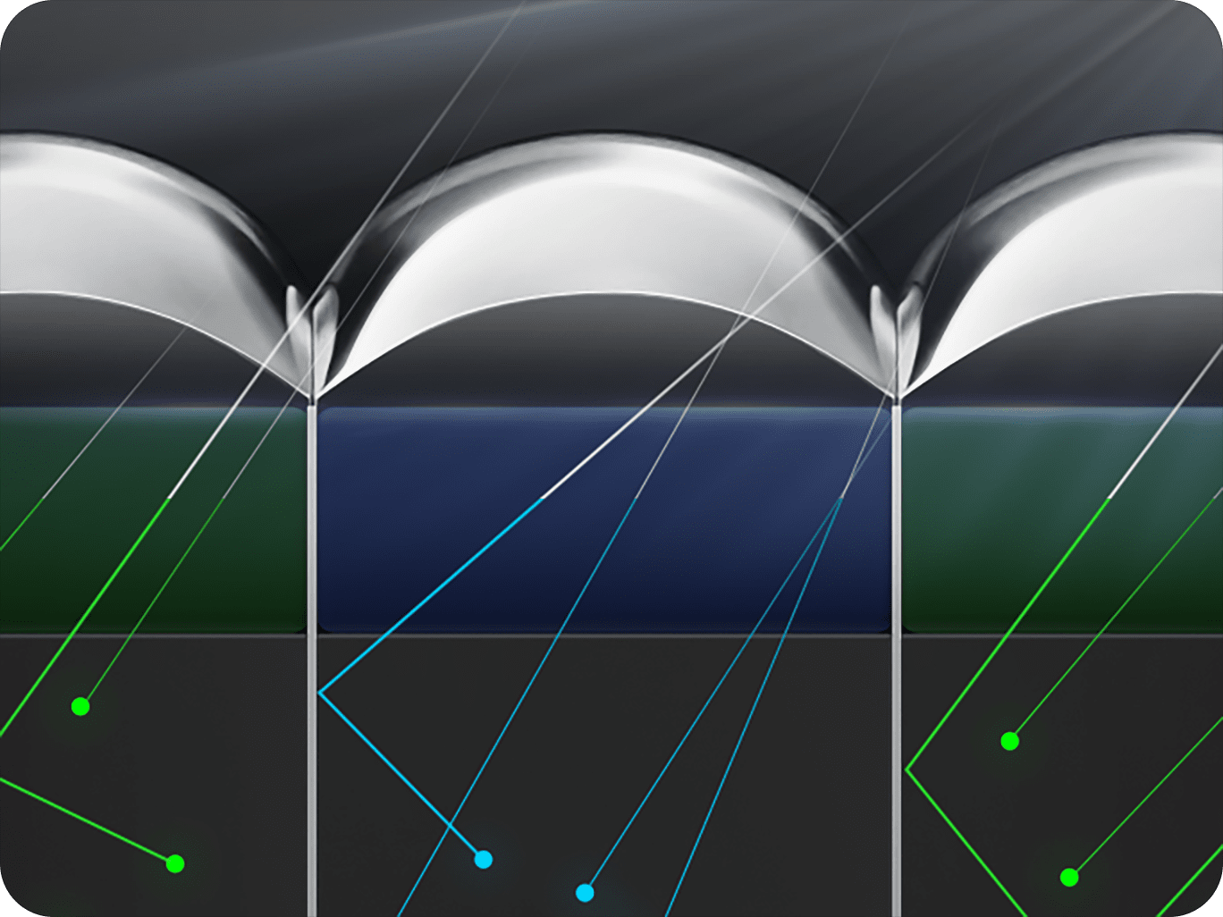
Samsung’s Nanoprism technology replaces the pixel's microlens with a nano-structured high-refractive-index material, utilizing the prism effect that occurs as light passes through it to capture more light. Since image sensor pixels have predefined RGB color filters, each pixel only accepts light that matches its designated color to pass through to the photodiode, filtering out the other light.
This is how Nanoprism works on a technical level: The high-refractive-index material separates light by wavelength as it passes through and then optimizes the optical path so that each wavelength is directed toward its corresponding color filter. This results in an approximately 25% improvement in light-gathering efficiency compared to traditional microlenses.2


Products for superior detail and color, day or night
Products for superior detail and color, day or night
Products for superior detail and color, day or night
