A place where your imagination
is fabricated into reality
A place where your imagination
is fabricated into reality
A place where your imagination
is fabricated into reality


Samsung Foundry Business Samsung Foundry Business Samsung Foundry Business
Samsung Foundry retains deep expertise in manufacturing system semiconductors for customers. We aim to become a ‘Total Foundry’, not only drawing on our state-of-the-art process technologies to produce chips for global fabless clients but also providing comprehensive solutions through our Library/PDK (Process Design Kit)/DM (Design Methodology)/Design Service infrastructure. We are preparing to bring innovative technologies to the market faster by producing high-quality products as efficiently as possible through state-of-the-art production facility automation. Samsung Foundry retains deep expertise in manufacturing system semiconductors for customers. We aim to become a ‘Total Foundry’, not only drawing on our state-of-the-art process technologies to produce chips for global fabless clients but also providing comprehensive solutions through our Library/PDK (Process Design Kit)/DM (Design Methodology)/Design Service infrastructure. We are preparing to bring innovative technologies to the market faster by producing high-quality products as efficiently as possible through state-of-the-art production facility automation. Samsung Foundry retains deep expertise in manufacturing system semiconductors for customers. We aim to become a ‘Total Foundry’, not only drawing on our state-of-the-art process technologies to produce chips for global fabless clients but also providing comprehensive solutions through our Library/PDK (Process Design Kit)/DM (Design Methodology)/Design Service infrastructure. We are preparing to bring innovative technologies to the market faster by producing high-quality products as efficiently as possible through state-of-the-art production facility automation.

Leading innovation and the future with Samsung Foundry Leading innovation and the future with Samsung Foundry Leading innovation and the future with Samsung Foundry
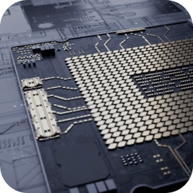
Samsung Foundry has made remarkable progress in semiconductor technology, reducing the process size from 28nm in 2012 to 3nm in 2022. We are constantly pushing the boundaries of semiconductor technology, providing a range of process technologies that offer significant improvements in power, performance, and scalability. From legacy processes to cutting-edge advanced processes, we are committed to taking chip performance to new heights across various industries. Samsung Foundry has made remarkable progress in semiconductor technology, reducing the process size from 28nm in 2012 to 3nm in 2022. We are constantly pushing the boundaries of semiconductor technology, providing a range of process technologies that offer significant improvements in power, performance, and scalability. From legacy processes to cutting-edge advanced processes, we are committed to taking chip performance to new heights across various industries. Samsung Foundry has made remarkable progress in semiconductor technology, reducing the process size from 28nm in 2012 to 3nm in 2022. We are constantly pushing the boundaries of semiconductor technology, providing a range of process technologies that offer significant improvements in power, performance, and scalability. From legacy processes to cutting-edge advanced processes, we are committed to taking chip performance to new heights across various industries.

Advanced and collaborative technologies Advanced and collaborative technologies Advanced and collaborative technologies
Samsung Foundry is focusing on developing cutting-edge under 3nm GAA (Gate All Around) process technology, accelerating the implementation of EUV process for mass production, and establishing a technological super-gap by developing state-of-the-art packaging technologies. In addition, the SAFE™ program enables competitive SoC design through cooperation between Samsung Foundry, partners, and customers. Samsung Foundry is focusing on developing cutting-edge under 3nm GAA (Gate All Around) process technology, accelerating the implementation of EUV process for mass production, and establishing a technological super-gap by developing state-of-the-art packaging technologies. In addition, the SAFE™ program enables competitive SoC design through cooperation between Samsung Foundry, partners, and customers. Samsung Foundry is focusing on developing cutting-edge under 3nm GAA (Gate All Around) process technology, accelerating the implementation of EUV process for mass production, and establishing a technological super-gap by developing state-of-the-art packaging technologies. In addition, the SAFE™ program enables competitive SoC design through cooperation between Samsung Foundry, partners, and customers.

Effective quality management Effective quality management Effective quality management
Samsung Foundry provides an efficient quality system and delivers the best products and services to meet customers’ requirements and expectations through a great quality management system, reliable supply chain security, and mass production quality control. Samsung Foundry provides an efficient quality system and delivers the best products and services to meet customers’ requirements and expectations through a great quality management system, reliable supply chain security, and mass production quality control. Samsung Foundry provides an efficient quality system and delivers the best products and services to meet customers’ requirements and expectations through a great quality management system, reliable supply chain security, and mass production quality control.

Samsung Foundry continues to lead the industry by innovating advanced process technologies across both mature and leading-edge nodes in the AI era.
Utilizing its heterogeneous integration technologies, Samsung Foundry provides advanced turnkey packaging services that meet the high-bandwidth, high-capacity, and low-power demands of the AI era.

With its SAFE™ partnership, Samsung Foundry has created the most trusted foundry ecosystem. Together with its partners, including IP, EDA, Cloud, DSP, OSAT, and MDI Alliance, Samsung Foundry optimizes the entire process from design to application-specific production. This enables tailored, advanced semiconductor development for our customers.
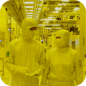
Samsung Foundry significantly improves production cycles and yields through smart fab operations and possesses flexible mass production capabilities for both legacy and next-generation advanced semiconductors based on our global foundry network.

Through dedicated teams for each customer and optimized Samsung AI solutions, Samsung Foundry provides process node options that meet the demands of various applications, such as HPC, mobile (5G), automotive, and IoT.