What is FinFET Technology?
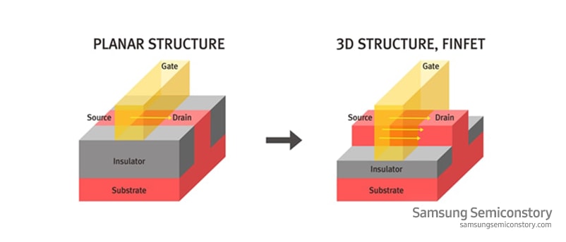
The FinFET (Fin Field Effect Transistor) process is a 3D process adopted to overcome the limitations of conventional planar (2D) structures. The structure looks like a fish’s fin, hence the name ‘Fin’FET. In a transistor, when voltage is applied to a gate, current flows through a channel from a ‘source’ to a ‘drain’. The broader the contact area between the gate and the channel is, the greater the efficiency is. In the FinFET process, a fin-shaped 3D structure is used to increase the contact area, thereby improving semiconductor performance and reducing leakage current.
Samsung Electronics has employed the FinFET process technology starting with its 14nm. In October 2016, Samsung became the first in the industry to mass produce 10nm FinFET semiconductors.
Our site uses cookies. We’d also like to set optional cookies to give you the best experience and provide you relevant advertising. you can choose to manage your preferences or accept all cookies. You can also read our Privacy Policy and Cookie Policy for more information.
This site uses cookies to personalise your experience, analyse site traffic. By Clicking Accept or continuing to browse the site you are agreeing to our use of cookies.
You can read our Privacy Policy and Cookie Policy for more information.
We use cookies to improve you experience on our website and to show you experience on our website and to show you relevant advertising, manage your settings for our cookies below.
These cookies are essential as they enable you to move around the website. This category cannot be disabled.
| Company | Domain |
|---|---|
| Samsung Electronics | semiconductor.samsung.com, image.semiconductor.samsung.com, smetrics.samsung.com |
These cookies collect information about how you use our website, for example which pages you visit most often. All information these cookies collect is used to improve how the website works.
| Cookie | Domain |
|---|---|
| ajax.googleapis.com, apis.google.com, calendar.google.com, developers.google.com, docs.google.com, google.com, maps.googleapis.com, spreadsheets.google.com, www.google.com, www.google.ie | |
| www.google-analytics.com, www.googletagmanager.com, www.gstatic.com | |
| Adobe | assets.adobedtm.com |
These cookies allow our website to remember choices you make (such as your user name, language or the region you are in) and tailor the website to provide enhanced features and content for you.
| Cookie | Domain | Purpose |
|---|---|---|
| Akamai | 176-34-86-175_s-23-203-249-81_ts-1604430438-clienttons-s.akamaihd.net, 176-34-86-175_s-23-203-249-81_ts-1604432488-clienttons-s.akamaihd.net, 176-34-86-175_s-23-203-249-90_ts-1604428164-clienttons-s.akamaihd.net, 176-34-86-175_s-95-101-143-18_ts-1604428258-clienttons-s.akamaihd.net, 176-34-86-175_s-95-101-143-24_ts-1604428321-clienttons-s.akamaihd.net, 34-242-207-243_s-23-203-249-81_ts-1604425495-clienttons-s.akamaihd.net, 34-242-207-243_s-23-203-249-81_ts-1604425563-clienttons-s.akamaihd.net, 34-242-207-243_s-23-203-249-81_ts-1604425669-clienttons-s.akamaihd.net, 34-242-207-243_s-23-203-249-81_ts-1604427540-clienttons-s.akamaihd.net, 34-242-207-243_s-23-203-249-81_ts-1604427617-clienttons-s.akamaihd.net, 34-242-207-243_s-23-203-249-81_ts-1604427664-clienttons-s.akamaihd.net, 34-242-207-243_s-23-203-249-81_ts-1604427922-clienttons-s.akamaihd.net, 34-242-207-243_s-23-203-249-81_ts-1604439090-clienttons-s.akamaihd.net, 34-242-207-243_s-23-203-249-81_ts-1604439174-clienttons-s.akamaihd.net, 34-242-207-243_s-23-203-249-81_ts-1604441206-clienttons-s.akamaihd.net, 34-242-207-243_s-23-203-249-81_ts-1604441267-clienttons-s.akamaihd.net, 34-242-207-243_s-23-203-249-90_ts-1604425484-clienttons-s.akamaihd.net, 34-242-207-243_s-23-203-249-90_ts-1604425610-clienttons-s.akamaihd.net, 34-242-207-243_s-23-203-249-90_ts-1604427737-clienttons-s.akamaihd.net, 34-242-207-243_s-23-203-249-90_ts-1604427797-clienttons-s.akamaihd.net, 34-242-207-243_s-23-203-249-90_ts-1604438922-clienttons-s.akamaihd.net, 34-242-207-243_s-23-203-249-90_ts-1604438968-clienttons-s.akamaihd.net, 34-242-207-243_s-23-203-249-90_ts-1604439033-clienttons-s.akamaihd.net, 34-242-207-243_s-23-203-249-90_ts-1604441023-clienttons-s.akamaihd.net, 34-242-207-243_s-95-101-129-82_ts-1604425732-clienttons-s.akamaihd.net, 34-245-202-11_s-23-203-249-81_ts-1604425513-clienttons-s.akamaihd.net, 34-245-202-11_s-23-203-249-81_ts-1604427569-clienttons-s.akamaihd.net, 34-245-202-11_s-23-203-249-90_ts-1604425365-clienttons-s.akamaihd.net, 34-246-182-217_s-23-203-249-81_ts-1604424915-clienttons-s.akamaihd.net, 34-246-182-217_s-23-203-249-81_ts-1604425000-clienttons-s.akamaihd.net, 34-246-182-217_s-23-203-249-81_ts-1604425155-clienttons-s.akamaihd.net, 34-246-182-217_s-23-203-249-81_ts-1604425567-clienttons-s.akamaihd.net, 34-246-182-217_s-23-203-249-81_ts-1604427446-clienttons-s.akamaihd.net, 34-246-182-217_s-23-203-249-81_ts-1604429495-clienttons-s.akamaihd.net, 34-246-182-217_s-23-203-249-90_ts-1604424817-clienttons-s.akamaihd.net, 34-246-182-217_s-23-203-249-90_ts-1604424939-clienttons-s.akamaihd.net, 34-246-182-217_s-23-203-249-90_ts-1604427359-clienttons-s.akamaihd.net, 34-246-182-217_s-23-203-249-90_ts-1604429563-clienttons-s.akamaihd.net, 34-246-182-217_s-95-101-129-82_ts-1604425062-clienttons-s.akamaihd.net, 34-246-182-217_s-95-101-143-18_ts-1604429398-clienttons-s.akamaihd.net, 34-246-182-217_s-95-101-143-24_ts-1604429274-clienttons-s.akamaihd.net, 34-246-182-217_s-95-101-143-24_ts-1604429365-clienttons-s.akamaihd.net, 34-246-182-217_s-95-101-143-24_ts-1604429616-clienttons-s.akamaihd.net, 364bf52c.akstat.io, 364bf5fa.akstat.io, 364bf6cc.akstat.io, 36c3fef2.akstat.io, 54-154-186-178_s-23-203-249-81_ts-1604425586-clienttons-s.akamaihd.net, 54-154-186-178_s-23-203-249-81_ts-1604429882-clienttons-s.akamaihd.net, 54-154-186-178_s-23-203-249-90_ts-1604425341-clienttons-s.akamaihd.net, 54-154-186-178_s-23-203-249-90_ts-1604425577-clienttons-s.akamaihd.net, 54-154-186-178_s-23-203-249-90_ts-1604425679-clienttons-s.akamaihd.net, 54-154-186-178_s-23-203-249-90_ts-1604427498-clienttons-s.akamaihd.net, 54-154-186-178_s-23-203-249-90_ts-1604431774-clienttons-s.akamaihd.net, 54-154-186-178_s-92-123-142-66_ts-1604427735-clienttons-s.akamaihd.net, 54-246-30-86_s-23-203-249-81_ts-1604425115-clienttons-s.akamaihd.net, 54-246-30-86_s-23-203-249-81_ts-1604427273-clienttons-s.akamaihd.net, 54-246-30-86_s-23-203-249-81_ts-1604427303-clienttons-s.akamaihd.net, 54-246-30-86_s-23-203-249-81_ts-1604427359-clienttons-s.akamaihd.net, 54-246-30-86_s-23-203-249-81_ts-1604431429-clienttons-s.akamaihd.net, 54-246-30-86_s-23-203-249-81_ts-1604431547-clienttons-s.akamaihd.net, 54-246-30-86_s-23-203-249-81_ts-1604435637-clienttons-s.akamaihd.net, 54-246-30-86_s-23-203-249-90_ts-1604427151-clienttons-s.akamaihd.net, 54-246-30-86_s-23-203-249-90_ts-1604429503-clienttons-s.akamaihd.net, 54-246-30-86_s-23-203-249-90_ts-1604429594-clienttons-s.akamaihd.net, 54-246-30-86_s-23-203-249-90_ts-1604433473-clienttons-s.akamaihd.net, 54-246-30-86_s-23-203-249-90_ts-1604433539-clienttons-s.akamaihd.net, 54-246-30-86_s-88-221-134-224_ts-1604435698-clienttons-s.akamaihd.net, 54-246-30-86_s-95-101-129-96_ts-1604424926-clienttons-s.akamaihd.net, 54-246-30-86_s-95-101-129-96_ts-1604424989-clienttons-s.akamaihd.net, 54-75-39-103_s-23-203-249-81_ts-1604425265-clienttons-s.akamaihd.net, 54-75-39-103_s-23-203-249-81_ts-1604425415-clienttons-s.akamaihd.net, 54-75-39-103_s-23-203-249-90_ts-1604425504-clienttons-s.akamaihd.net, 54-75-39-103_s-95-101-143-24_ts-1604432234-clienttons-s.akamaihd.net, 54-75-41-190_s-23-203-249-81_ts-1604424935-clienttons-s.akamaihd.net, 54-75-41-190_s-23-203-249-81_ts-1604425058-clienttons-s.akamaihd.net, 54-75-41-190_s-23-203-249-81_ts-1604425120-clienttons-s.akamaihd.net, 54-75-41-190_s-23-203-249-81_ts-1604425189-clienttons-s.akamaihd.net, 54-75-41-190_s-23-203-249-81_ts-1604427540-clienttons-s.akamaihd.net, 54-75-41-190_s-23-203-249-90_ts-1604424875-clienttons-s.akamaihd.net, 54-75-41-190_s-23-203-249-90_ts-1604425270-clienttons-s.akamaihd.net, 54-75-41-190_s-23-203-249-90_ts-1604427110-clienttons-s.akamaihd.net, 54-75-41-190_s-23-203-249-90_ts-1604429433-clienttons-s.akamaihd.net, 54-75-41-190_s-23-203-249-90_ts-1604429456-clienttons-s.akamaihd.net, 54-75-41-190_s-92-123-140-11_ts-1604427291-clienttons-s.akamaihd.net, 54-75-41-190_s-92-123-140-11_ts-1604427412-clienttons-s.akamaihd.net, 54-75-41-190_s-95-101-129-96_ts-1604425019-clienttons-s.akamaihd.net, 54-75-41-190_s-95-101-143-18_ts-1604429529-clienttons-s.akamaihd.net, 684dd305.akstat.io, 684dd306.akstat.io, 684dd307.akstat.io, 684dd308.akstat.io, 684dd309.akstat.io, 684dd30a.akstat.io, 684dd30c.akstat.io, 684dd30d.akstat.io, 6852bd07.akstat.io, 6852bd08.akstat.io, 6852bd09.akstat.io, 6852bd0a.akstat.io, 6852bd0b.akstat.io, 6852bd0c.akstat.io, 6852bd0d.akstat.io, 6852bd0e.akstat.io, 6852bd0f.akstat.io, 6852bd10.akstat.io, 6852bd11.akstat.io, 6852bd12.akstat.io, 6852bd13.akstat.io, 6852bd14.akstat.io, 685d5b18.akstat.io, 685d5b19.akstat.io, 685d5b1b.akstat.io, 686eb51b.akstat.io, 686eb704.akstat.io, bcsecure01-a.akamaihd.net, brightcove04pmdo-a.akamaihd.net, ds-aksb-a.akamaihd.net, el24ucyccuqvax5bs2kq-pblhb6-a723eeea5-clientnsv4-s.akamaihd.net, el24ucyccuqvax5bt4yq-ptbmxa-6ef8e4803-clientnsv4-s.akamaihd.net, el24ucyccuqwcx5bs4uq-p03zy7-676237e5e-clientnsv4-s.akamaihd.net, el3lnwiccuqvax5bstvq-pch0tk-1cdf76638-clientnsv4-s.akamaihd.net, el3lnwiccuqvax5buy2q-pqnfkn-f673b4feb-clientnsv4-s.akamaihd.net, el3lnwiccuqvax5buzkq-pl30i3-08d7d87df-clientnsv4-s.akamaihd.net, el3lnwiccuqwcx5bu4ya-pyg66y-cb19a994e-clientnsv4-s.akamaihd.net, el3lnwiccuqxax5bstjq-puyi2b-1f022524f-clientnsv4-s.akamaihd.net, el3lnwiccuqxax5bsuua-pioden-695058c8f-clientnsv4-s.akamaihd.net, el3lnwiccuqxax5bsvta-pqns0s-b6979dbf5-clientnsv4-s.akamaihd.net, el3lnwiccuqxax5btzpq-pbifp1-07760bdf0-clientnsv4-s.akamaihd.net, el3lnwiccuqxax5bu23q-p2ez1a-7d289db29-clientnsv4-s.akamaihd.net, el3lnwixzp4swx5bs5pq-pnfw20-03cb87b70-clientnsv4-s.akamaihd.net, el3lnwixzp4swx5bsryq-p52tb9-f3dab0dd0-clientnsv4-s.akamaihd.net, el3lnwixzp4swx5bu35q-pdannf-fd1139023-clientnsv4-s.akamaihd.net, el3lnwixzp4swx5buxna-pyccr1-f710a073b-clientnsv4-s.akamaihd.net, el3lnwky3wdkax5bsxbq-p3hn9l-a2a7437e4-clientnsv4-s.akamaihd.net, el3lnwky3wdkex5bt23a-pfcryk-8b7c1430e-clientnsv4-s.akamaihd.net, elzm742y3wdkex5bs4lq-p0p40d-3a2e745b5-clientnsv4-s.akamaihd.net, elzm742y3wdkex5bzofa-pqb527-96b6b1fc9-clientnsv4-s.akamaihd.net, elzm74yccuqvax5b2szq-pf5z0b-8e0fe713e-clientnsv4-s.akamaihd.net, elzm74yccuqvax5bs5nq-pt4puj-60e29ce0a-clientnsv4-s.akamaihd.net, elzm74yccuqvax5bzo4a-ptxi68-223a872ab-clientnsv4-s.akamaihd.net, elzm74yccuqwcx5b2r3a-p84t0a-b5b6d0cb9-clientnsv4-s.akamaihd.net, elzm74yccuqwcx5btaca-p2p13t-2edd5f4d6-clientnsv4-s.akamaihd.net, elzm74yccuqwcx5buakq-p7s1ie-7095e2510-clientnsv4-s.akamaihd.net, elzm74yccuqxax5b2o7q-partxm-0ba99e22d-clientnsv4-s.akamaihd.net, elzm74yccuqxax5bs6fa-pnivpg-c492934bb-clientnsv4-s.akamaihd.net, elzm74yccuqxax5bt5qq-pcrjf9-bdc24fa26-clientnsv4-s.akamaihd.net, elzm74yccuqxax5bzp4q-pkl6rx-fb475a90e-clientnsv4-s.akamaihd.net, elzm74yxzp4swx5bs4ga-p9xzbs-ed47165ae-clientnsv4-s.akamaihd.net, elzm74yxzp4swx5bs7cq-p4s4el-cd1a19887-clientnsv4-s.akamaihd.net, elzm74yxzp4swx5bt4ka-p0qvim-2e8a5e71e-clientnsv4-s.akamaihd.net, elzm74yxzp4swx5bt6hq-pzy1yp-35d9d01e0-clientnsv4-s.akamaihd.net, elzm74yxzp4swx5bt7mq-p1duy0-1060998fa-clientnsv4-s.akamaihd.net, elzm74yxzp4swx5bucja-p0twy9-19851792c-clientnsv4-s.akamaihd.net, elzm74yxzp4swx5bzqza-pn76ir-1c0c55ff7-clientnsv4-s.akamaihd.net, elzm74yxzp4swx5bzsda-pqodge-888ec876f-clientnsv4-s.akamaihd.net, g2nlvmqcchiscx5bva5a-pwotro-14b66ca5a-clientnsv4-s.akamaihd.net, g2nlvmqccuqvax5bs7hq-p4vzcl-ad59a5fd9-clientnsv4-s.akamaihd.net, g2nlvmqccuqxax5bsz6q-pm3a6a-3feb7d021-clientnsv4-s.akamaihd.net, g2nlvmqxzp4swx5bs5uq-pd12b9-62c8cb38d-clientnsv4-s.akamaihd.net, g2nlvmqxzp4swx5bt3va-p7puv0-d4fafcfea-clientnsv4-s.akamaihd.net, g2nlvmsy3wdkax5bs5zq-p675cj-d0b1fd299-clientnsv4-s.akamaihd.net, g33b4vqccuqvax5btwhq-pfp8ei-5c0ea4329-clientnsv4-s.akamaihd.net, g33b4vqccuqvax5btytq-pupet4-0083df35c-clientnsv4-s.akamaihd.net, g33b4vqccuqvax5btzpq-pr1f2f-01d5fb765-clientnsv4-s.akamaihd.net, g33b4vqccuqvax5bvzcq-phk9tj-828709858-clientnsv4-s.akamaihd.net, g33b4vqccuqvax5bw2bq-py1x2v-a7310f6e5-clientnsv4-s.akamaihd.net, g33b4vqccuqvax5bx3za-pge3ox-a91a32353-clientnsv4-s.akamaihd.net, g33b4vqccuqwcx5bu4na-pqdvvi-3aaa5c611-clientnsv4-s.akamaihd.net, g33b4vqccuqwcx5bwzaq-pvw5k6-d3e3dcd05-clientnsv4-s.akamaihd.net, g33b4vqccuqwcx5bx22q-p8kovq-e038e0c0c-clientnsv4-s.akamaihd.net, g33b4vqccuqxax5bstpa-p4rsfx-bd0382a30-clientnsv4-s.akamaihd.net, g33b4vqccuqxax5btyeq-poz8cc-9955b8a36-clientnsv4-s.akamaihd.net, g33b4vqxzp4swx5bu27q-pxv1vf-89db7a111-clientnsv4-s.akamaihd.net, g33b4vqxzp4swx5bv25q-pt8447-731cc407d-clientnsv4-s.akamaihd.net, g33b4vsy3wdkax5bswnq-plqmrf-ff7289811-clientnsv4-s.akamaihd.net, g33b4vsy3wdkex5bsuoq-p56ka1-9bf23f300-clientnsv4-s.akamaihd.net, gzfsozyccuqwcx5bs3dq-p2yzo8-69eb1f4d7-clientnsv4-s.akamaihd.net, gzfsozyccuqwcx5bs4qa-p299q7-a9521f4ee-clientnsv4-s.akamaihd.net, gzfsozyccuqwcx5bsyyq-pv69oz-aed1b09c6-clientnsv4-s.akamaihd.net, gzfsozyccuqwcx5bwfuq-pw4gfb-c2c42381f-clientnsv4-s.akamaihd.net, gzfstpqccuqvax5bssvq-p0x8hm-7a3d7367f-clientnsv4-s.akamaihd.net, gzfstpqccuqvax5bsxsq-p2oajs-b2e67f00b-clientnsv4-s.akamaihd.net, gzfstpqccuqvax5bsy3a-pfuzjd-60f8ba5de-clientnsv4-s.akamaihd.net, gzfstpqccuqvax5bu2ia-p6uwyn-30e7a92df-clientnsv4-s.akamaihd.net, gzfstpqccuqwcx5bswqa-pplxq4-ee58ceb89-clientnsv4-s.akamaihd.net, gzfstpqccuqwcx5bu3mq-p6qff7-f4c4075e7-clientnsv4-s.akamaihd.net, gzfstpqccuqwcx5buz4q-pbk4m8-d20c90e54-clientnsv4-s.akamaihd.net, gzfstpqccuqxax5bt4ka-p3fi1s-1fcad7cd5-clientnsv4-s.akamaihd.net, gzfstpqxzp4swx5bsttq-p683qt-2c3f6e21e-clientnsv4-s.akamaihd.net, gzfstpqxzp4swx5bsu5q-pyioyl-3b5424f35-clientnsv4-s.akamaihd.net, gzfstpqxzp4swx5bsvra-ps8whv-800c4ca06-clientnsv4-s.akamaihd.net, gzfstpqxzp4swx5bt2ka-p3owfu-9bef421db-clientnsv4-s.akamaihd.net, gzfstpqxzp4swx5btynq-p80cg4-5fbda6ae3-clientnsv4-s.akamaihd.net, gzfstpsy3wdkax5btvta-pc4hb3-c24fbde0b-clientnsv4-s.akamaihd.net, i03f9f400-ds-aksb-a.akamaihd.net, i03fa4400-ds-aksb-a.akamaihd.net, i03faac00-ds-aksb-a.akamaihd.net, i03fae300-ds-aksb-a.akamaihd.net, i03fb4f00-ds-aksb-a.akamaihd.net, i22f29600-ds-aksb-a.akamaihd.net, i22f44600-ds-aksb-a.akamaihd.net, i22f47c00-ds-aksb-a.akamaihd.net, i22f4a100-ds-aksb-a.akamaihd.net, i22f55c00-ds-aksb-a.akamaihd.net, i22f5ca00-ds-aksb-a.akamaihd.net, i22f6b100-ds-aksb-a.akamaihd.net, i22f7bf00-ds-aksb-a.akamaihd.net, i22fdb800-ds-aksb-a.akamaihd.net, i22fdd700-ds-aksb-a.akamaihd.net, i3430c200-ds-aksb-a.akamaihd.net, i34d04400-ds-aksb-a.akamaihd.net, i34d71700-ds-aksb-a.akamaihd.net, i36486200-ds-aksb-a.akamaihd.net, i364b2700-ds-aksb-a.akamaihd.net, i369aba00-ds-aksb-a.akamaihd.net, i36d85900-ds-aksb-a.akamaihd.net, i36d86800-ds-aksb-a.akamaihd.net, i36e56b00-ds-aksb-a.akamaihd.net, i36f61e00-ds-aksb-a.akamaihd.net, i36f6c000-ds-aksb-a.akamaihd.net, i3f23f800-ds-aksb-a.akamaihd.net, ib0225600-ds-aksb-a.akamaihd.net, s.go-mpulse.net, trial-eum-clientnsv4-s.akamaihd.net, trial-eum-clienttons-s.akamaihd.net, warfnl2y3wdkex5buhra-pvnsej-42dd2535b-clientnsv4-s.akamaihd.net, warfnlyccuqvax5bvjta-pivu9l-324052216-clientnsv4-s.akamaihd.net, warfnlyccuqxax5bwjua-pt5xj8-63e5f59c4-clientnsv4-s.akamaihd.net, warfnlyxzp4swx5bugca-p9ihiy-2a56daf9f-clientnsv4-s.akamaihd.net, warfnlyxzp4swx5buiqq-p5eemy-20706e9d7-clientnsv4-s.akamaihd.net To provide the optimized image quality and enhance page loading speed | To provide the optimized image quality and enhance page loading speed |
| Amazon (Cloud Front) |
Amazon (Cloud Front) d15mv1adrb1s6e.cloudfront.net, d1vp9jkpfdwr15.cloudfront.net, d25jv1xpupcva6.cloudfront.net, d2cmqkwo8rxlr9.cloudfront.net, d2m3ikv8mpgiy8.cloudfront.net, d334tbn9icrqnt.cloudfront.net, d38nbbai6u794i.cloudfront.net, d3dvvd5arbl3b4.cloudfront.net, d3nkfb7815bs43.cloudfront.net, d9qz450atvita.cloudfront.net To speed up the delivery of your static content (e.g., images, style sheets, JavaScript, etc.) to viewers across the globe | To speed up the delivery of your static content (e.g., images, style sheets, JavaScript, etc.) to viewers across the globe |
| Brightcove | admin.brightcove.com, metrics.brightcove.com, players.brightcove.net, sadmin.brightcove.com, vjs.zencdn.net | To support video streaming |
These cookies gather information about your browser habits. They remember that you've visited our website and share this information with other organizations such as advertisers.
| Cookie | Domain |
|---|---|
| atdmt.com, connect.facebook.net, cx.atdmt.com, facebook.com, www.facebook.com | |
| Google Advertising | ad.doubleclick.net, adservice.google.com, adservice.google.ie, cm.g.doubleclick.net, doubleclick.net, googleads.g.doubleclick.net, pubads.g.doubleclick.net, static.doubleclick.net, stats.g.doubleclick.net, www.googleadservices.com |
| s.ytimg.com, www.youtube.com, youtube.com | |
| ads.linkedin.com, linkedin.com, px.ads.linkedin.com, www.linkedin.com |
Cookies are small files that store information on your computer, TV, mobile phone, or other device. They enable the entity that put the cookie on your device to recognize you across different websites, services, devices, and/or browsing sessions.