

Samsung Semiconductor has developed a variety of products that have received carbon reduction certifications. What kinds of activities is Samsung Semiconductor currently undertaking to reduce its environmental impact?
Samsung Semiconductor has developed a variety of products that have received carbon reduction certifications. What kinds of activities is Samsung Semiconductor currently undertaking to reduce its environmental impact?
Samsung Semiconductor has developed a variety of products that have received carbon reduction certifications. What kinds of activities is Samsung Semiconductor currently undertaking to reduce its environmental impact?
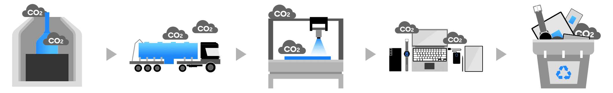
Life Cycle Assessment (LCA) is a method used to collectively evaluate a product’s environmental impact through its’ entire life cycle from its raw materials extraction stage to production, application and disposal of a product. However, adopting the methods on semiconductor has been a continuing challenge as it requires numerous raw material, hundreds of complicated manufacturing processes and thousands of application. However, after strenuous studies and research, Samsung Semiconductor came up with a comprehensive way to accounts the vast amount of necessary data to measure carbon emitted throughout semiconductor’s lifecycle. As a result, 38 Samsung’s semiconductors received Product Carbon Footprint (PCF) certification by The Carbon Trust using this assessment. Take a look at our PCF certified products that delineate Samsung Electronics’ eco-friendly footprint and reflect our continuous effort to protect the environment *The Carbon Trust is an eco-friendly certification non-profit organization established in 2001 by the British government. The Carbon Trust awards carbon footprint and water footprint certifications in accordance with international inspection standards, by comprehensively measuring the environmental impact of the consumption of carbon and water, from the pre-production stage to the entire production process of a product.
Life Cycle Assessment (LCA) is a method used to collectively evaluate a product’s environmental impact through its’ entire life cycle from its raw materials extraction stage to production, application and disposal of a product. However, adopting the methods on semiconductor has been a continuing challenge as it requires numerous raw material, hundreds of complicated manufacturing processes and thousands of application. However, after strenuous studies and research, Samsung Semiconductor came up with a comprehensive way to accounts the vast amount of necessary data to measure carbon emitted throughout semiconductor’s lifecycle. As a result, 38 Samsung’s semiconductors received Product Carbon Footprint (PCF) certification by The Carbon Trust using this assessment. Take a look at our PCF certified products that delineate Samsung Electronics’ eco-friendly footprint and reflect our continuous effort to protect the environment *The Carbon Trust is an eco-friendly certification non-profit organization established in 2001 by the British government. The Carbon Trust awards carbon footprint and water footprint certifications in accordance with international inspection standards, by comprehensively measuring the environmental impact of the consumption of carbon and water, from the pre-production stage to the entire production process of a product.
Life Cycle Assessment (LCA) is a method used to collectively evaluate a product’s environmental impact through its’ entire life cycle from its raw materials extraction stage to production, application and disposal of a product. However, adopting the methods on semiconductor has been a continuing challenge as it requires numerous raw material, hundreds of complicated manufacturing processes and thousands of application. However, after strenuous studies and research, Samsung Semiconductor came up with a comprehensive way to accounts the vast amount of necessary data to measure carbon emitted throughout semiconductor’s lifecycle. As a result, 38 Samsung’s semiconductors received Product Carbon Footprint (PCF) certification by The Carbon Trust using this assessment. Take a look at our PCF certified products that delineate Samsung Electronics’ eco-friendly footprint and reflect our continuous effort to protect the environment *The Carbon Trust is an eco-friendly certification non-profit organization established in 2001 by the British government. The Carbon Trust awards carbon footprint and water footprint certifications in accordance with international inspection standards, by comprehensively measuring the environmental impact of the consumption of carbon and water, from the pre-production stage to the entire production process of a product.


first to obtain
in the industry
→
UFS
(1 type)
Expansion of key
memory products
→
DRAM/SSD/
Memory card
(8 types)
Expansion of system semiconductors
and
memory
products in 2021
→
Logic chips (3 types)/
Image sensor (1 type)/
DRAM/SSD/Memory
card(20 types)

first to obtain
in the industry
→
UFS
(1 type)
Expansion of
memory products
→
DRAM/SSD/UFS/
Memory card
(5
types)
* Carbon Trust certified products expire 2 years after the date of certification acquisition
Samsung Semiconductor, the first in the semiconductor industry to receive CO₂ measured label and reducing CO₂ label awarded by the Carbon Trust, obtained the Product Carbon Footprint certification (CO₂ measured label) for 1 type of UFS in 2019, DRAM, SSD, and 8 types of memory cards in 2020, 4 types of system semiconductors, DRAM, SSD and 20 types of memory cards in 2021. Reducing CO₂ label can be obtained if the follow-up model of a product with carbon footprint certification reduces its carbon emissions in comparison to the existing model. In 2020, Samsung Semiconductor obtained a reducing CO₂ label for one type of UFS that had been awarded carbon footprint certification in 2019 for the first time in the industry. In addition to this, in 2021, DRAM, SSD, UFS, and five types of memory cards also received the reducing label.
Samsung Semiconductor, the first in the semiconductor industry to receive CO₂ measured label and reducing CO₂ label awarded by the Carbon Trust, obtained the Product Carbon Footprint certification (CO₂ measured label) for 1 type of UFS in 2019, DRAM, SSD, and 8 types of memory cards in 2020, 4 types of system semiconductors, DRAM, SSD and 20 types of memory cards in 2021. Reducing CO₂ label can be obtained if the follow-up model of a product with carbon footprint certification reduces its carbon emissions in comparison to the existing model. In 2020, Samsung Semiconductor obtained a reducing CO₂ label for one type of UFS that had been awarded carbon footprint certification in 2019 for the first time in the industry. In addition to this, in 2021, DRAM, SSD, UFS, and five types of memory cards also received the reducing label.
Samsung Semiconductor, the first in the semiconductor industry to receive CO₂ measured label and reducing CO₂ label awarded by the Carbon Trust, obtained the Product Carbon Footprint certification (CO₂ measured label) for 1 type of UFS in 2019, DRAM, SSD, and 8 types of memory cards in 2020, 4 types of system semiconductors, DRAM, SSD and 20 types of memory cards in 2021. Reducing CO₂ label can be obtained if the follow-up model of a product with carbon footprint certification reduces its carbon emissions in comparison to the existing model. In 2020, Samsung Semiconductor obtained a reducing CO₂ label for one type of UFS that had been awarded carbon footprint certification in 2019 for the first time in the industry. In addition to this, in 2021, DRAM, SSD, UFS, and five types of memory cards also received the reducing label.


