Samsung Electronics participated in FMS 2026 (Future of Memory and Storage), held from August 4 to 6 at the Santa Clara Convention Center in California, where the company showcased innovative memory and storage technologies for next-generation AI systems and presented its vision for 3D Memory Architecture, outlining a new direction for AI memory and storage infrastructure.
FMS is a global industry event that has evolved around memory and storage technologies. Marking its 20th anniversary this year, the event further strengthened its identity as a business platform encompassing AI systems and data center infrastructure, expanding beyond its traditional focus on flash memory. Memory and storage manufacturers, along with a wide range of AI companies, participated in the event to share next-generation technologies and discuss the future direction of the industry.
Following last year’s participation, Samsung once again joined the event as an Executive Premier sponsor, the highest sponsorship tier. Under the theme “Architecting AI Systems – Innovations. Together.” Samsung focused on next-generation 3D memory and storage architecture innovations designed to improve the performance and efficiency of AI systems.

Next-generation AI architecture vision based on 3D innovation
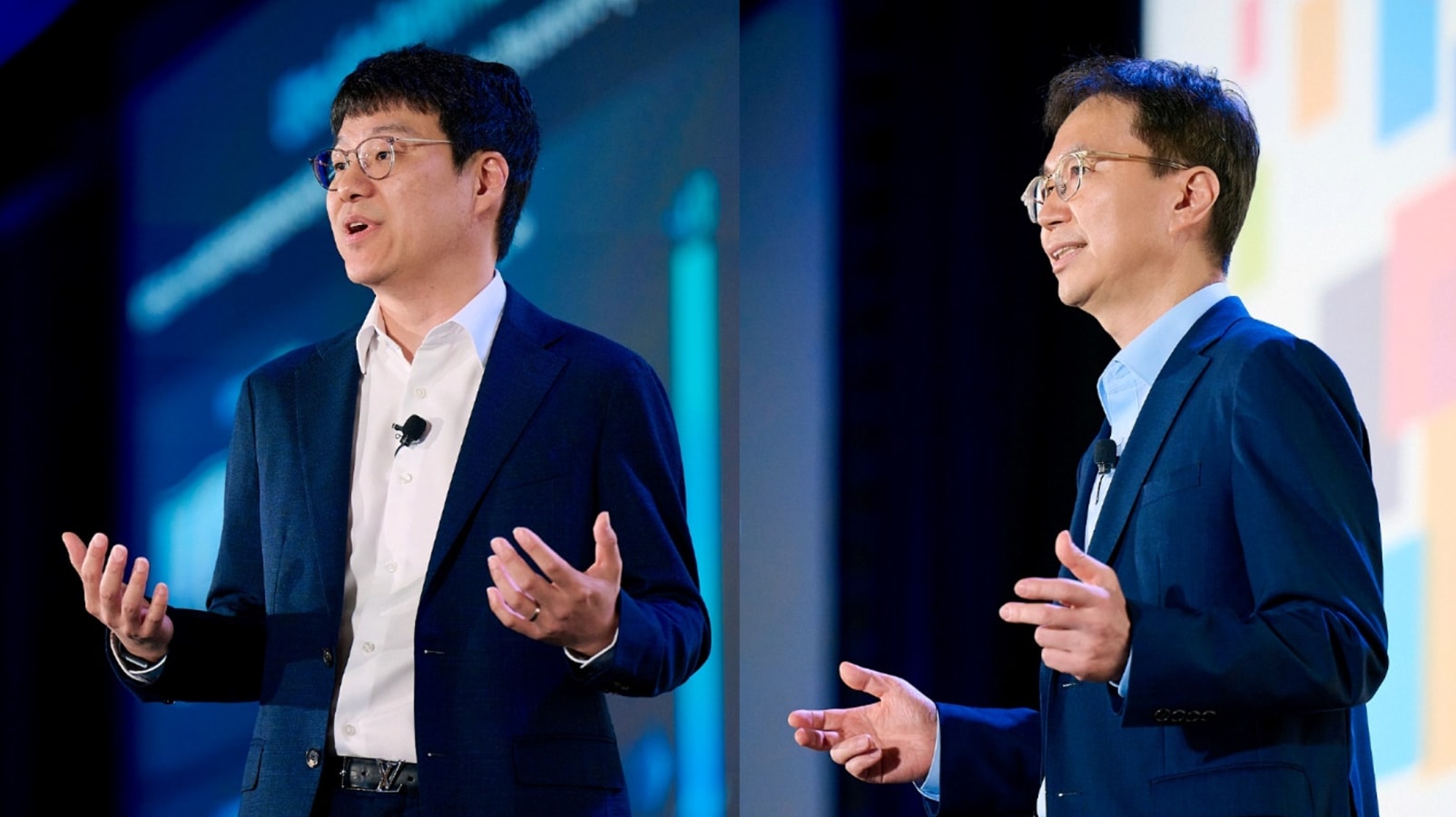
During Samsung’s keynote, Jin-yub Lee, EVP of Flash Development, and Kyung-ryun Kim, VP of DRAM Development, presented next-generation technologies including zHBM, zNAND-O, and V10 BV-NAND under the theme “3D Innovations in Memory & Storage Architecture.” They also introduced Samsung’s vision for 3D architecture as a way to address the rapidly growing bottlenecks in AI infrastructure.
As AI models and computing performance continue to grow rapidly, increasing input context lengths and KV cache sizes are driving sustained demand for greater memory bandwidth and capacity. At the same time, system power consumption, heat generation, latency caused by data movement, and energy consumption are emerging as major constraints on the expansion of AI infrastructure.
As a result, simply increasing the speed or capacity of individual memory products is no longer sufficient to meet system-level requirements. Samsung presented 3D architecture, which vertically connects and integrates logic, memory, and storage, as a key technology direction for overcoming these limitations.
① HBM transforming AI system performance
In the DRAM segment, Samsung introduced its HBM roadmap, including next-generation HBM4E and HBM5, which combines leading-edge DRAM processes, TSV-based stacking structures, and advanced packaging technologies to continuously improve bandwidth, capacity, and power efficiency.
In particular, Samsung unveiled zHBM, a next-generation AI memory architecture, at the event.
zHBM is a next-generation solution that integrates logic and memory in 3D to reduce the physical distance data must travel and alleviate data movement bottlenecks found in conventional systems. Through this approach, it aims to achieve the high memory performance and energy efficiency required by AI systems.
With zHBM, Samsung presented a next-generation AI system design direction that goes beyond continuously increasing HBM bandwidth by innovating the placement and interconnection architecture of logic and memory itself.
② Next-generation NAND and storage strategy optimized for AI workloads
In the NAND segment, Samsung introduced next-generation NAND technologies and a product portfolio designed to support diverse AI data center workloads.
The PCIe Gen6 TLC SSD PM1763, based on V9 V-NAND, supports the high data processing performance and reliability required for AI training and inference. PCIe Gen5 QLC SSDs provide high density and cost efficiency for environments that require large-scale data storage.
Samsung presented a storage strategy that optimizes both AI infrastructure performance and total cost of ownership by deploying TLC-based SSDs for performance-intensive data and QLC-based SSDs for high-capacity storage.
Samsung also unveiled V10, which applies next-generation wafer bonding technology. V10 is a next-generation NAND product that delivers higher performance and power efficiency through an ultra-high-layer structure of more than 400 layers.
Samsung also introduced zNAND-O as a key next-generation solution. zNAND-O is a next-generation high-performance NAND flash developed by Samsung. It advances the vertical stacking technology of conventional V-NAND and applies 3D packaging to four or eight semiconductor dies. Optimized for edge AI, it delivers high performance in environments that require real-time processing of large-scale data.
NVIDIA special session
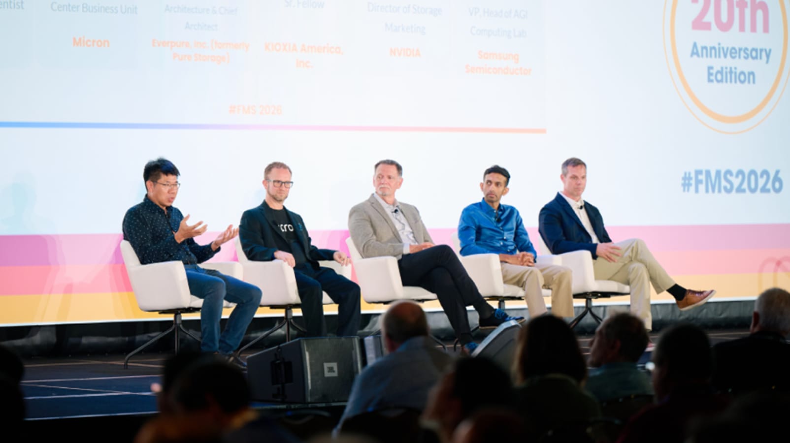
During FMS, Samsung participated not only in the keynote but also in a special session hosted by NVIDIA and technical sessions organized by FMS, sharing its perspective on the future direction of memory and storage technologies in the AI era and discussing opportunities for industry collaboration.
Yang Seok Ki, Vice President of the AGI Computing Lab, participated in NVIDIA’s executive session, “Balancing Memory and Storage to Operate AI Factories and Agents at Scale,” where he highlighted the importance of optimizing data placement across memory and storage tiers based on their respective characteristics to improve the operational efficiency of AI factories.
Samsung also participated in a total of 20 sessions in the official FMS conference program, sharing a range of technologies with industry professionals.
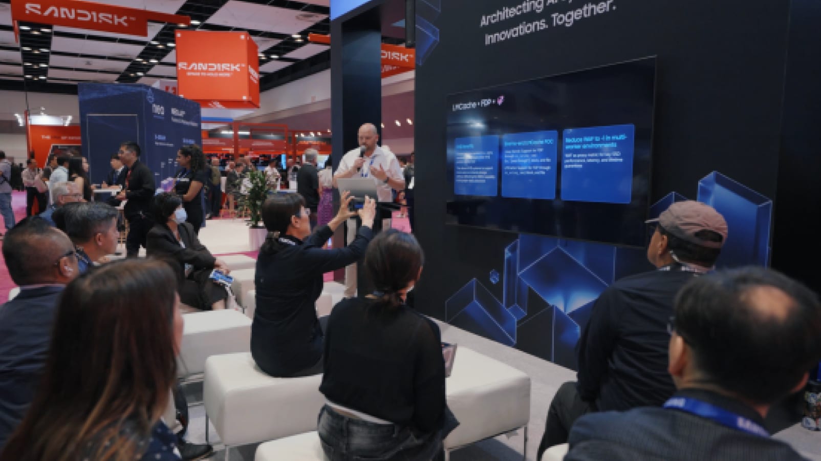
At the Samsung booth, approximately 10 mini-theater sessions were held to provide more detailed explanations of the 3D architecture vision and next-generation products and technologies introduced during the keynote, while expanding on-site engagement with customers and ecosystem partners.
Total memory and storage solutions spanning cloud AI and edge AI
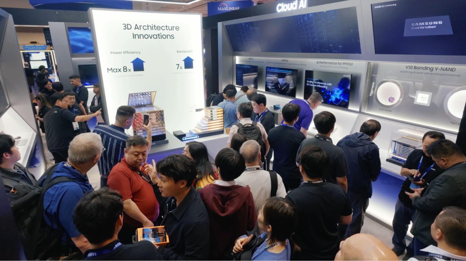
Samsung’s exhibition booth was organized into several areas, including a Highlight Zone, a Cloud AI Zone, and an Edge AI Zone.
In the Highlight Zone, Samsung used mock-ups and demonstrations to present the concepts of zHBM, which vertically connects logic and memory, and zNAND-O, which integrates high-performance NAND in 3D. The zone was designed to help visitors intuitively understand next-generation 3D memory and storage structures and their roles within systems.
The Cloud AI Zone featured high-performance, high-capacity memory and storage solutions for large-scale AI data centers and accelerated computing environments, including ▲ next-generation HBM ▲ CMM-D MD310 ▲ PM1763 ▲ BM1773.
The Edge AI Zone showcased low-power, high-performance solutions for edge AI environments, including ▲ LPDDR5X-PIM ▲ LPDDR6 ▲ UFS 5.0.
A wall display within the exhibition area brought together Samsung’s memory and storage portfolio for Cloud AI, Edge AI, and Physical AI, allowing visitors to see at a glance the company’s broad solution capabilities for supporting diverse AI environments.
Two categories winning at the FMS 2026 Best of Show Awards
Samsung was recognized for its next-generation memory and storage technologies by winning in two categories at the FMS 2026 Best of Show Awards.
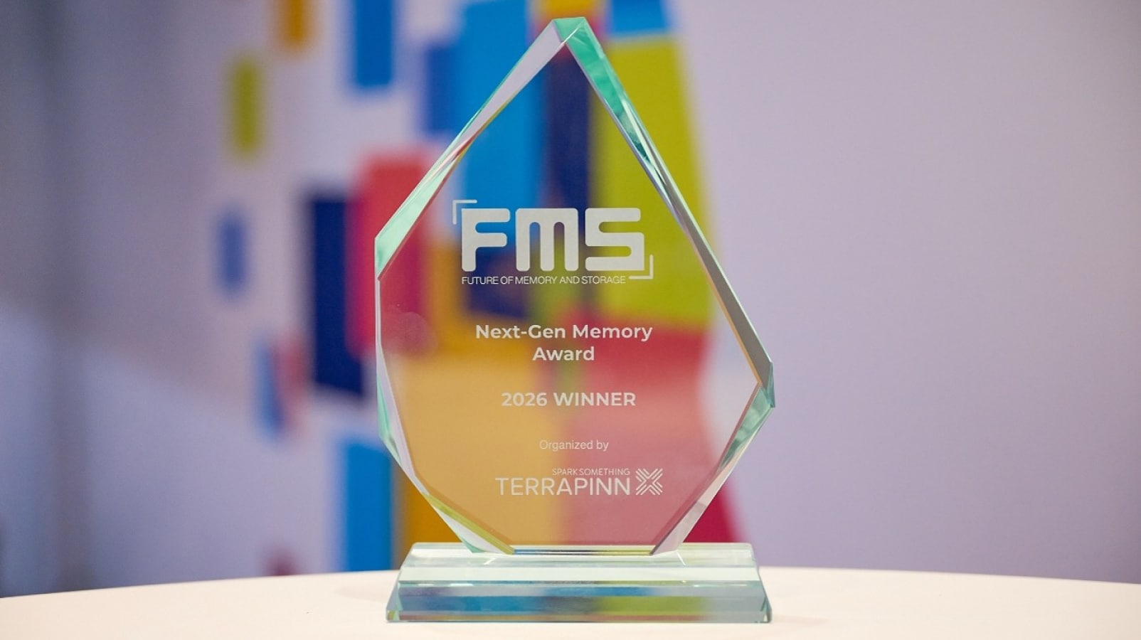
V10 BV-NAND received the 3D & Innovation Award, while LPDDR5X-PIM received the Next-Gen Memory Award.
V10 BV-NAND was recognized for its innovative characteristics, including the application of next-generation wafer bonding technology, ultra-high-layer integration, high performance, and low power consumption. LPDDR5X-PIM received strong evaluations for providing a low-power, high-performance design that enables efficient AI model inference.
These awards demonstrate Samsung’s broad competitiveness in memory and storage technologies supporting diverse AI environments, from cloud to edge.
Samsung’s comprehensive semiconductor capabilities advancing 3D architecture
Innovation in AI systems can no longer be achieved solely through performance improvements in individual memory or storage products. To translate improvements in computing performance into actual system-level gains, challenges related to memory bandwidth and capacity, data movement, power delivery, and heat generation must be addressed together.
3D architecture is a key technology direction for solving these challenges. Implementing next-generation 3D architecture requires leading-edge memory processes, high-performance logic, die-to-die interconnects, power delivery, thermal management, and advanced packaging technologies to be designed together from a system-level perspective.
As a comprehensive semiconductor company with capabilities across memory, logic, foundry, and advanced packaging, Samsung is able to design and optimize these complex technology elements in an integrated manner. These end-to-end capabilities provide a differentiated foundation for improving not only the performance and power efficiency of next-generation memory and storage products, but also the overall completeness of systems.
Samsung will continue to advance memory and storage innovation through close collaboration with customers and ecosystem partners, while further strengthening its semiconductor technology leadership in the AI era based on its end-to-end solution capabilities.

 Global