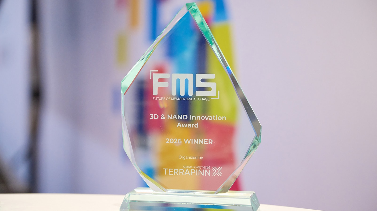
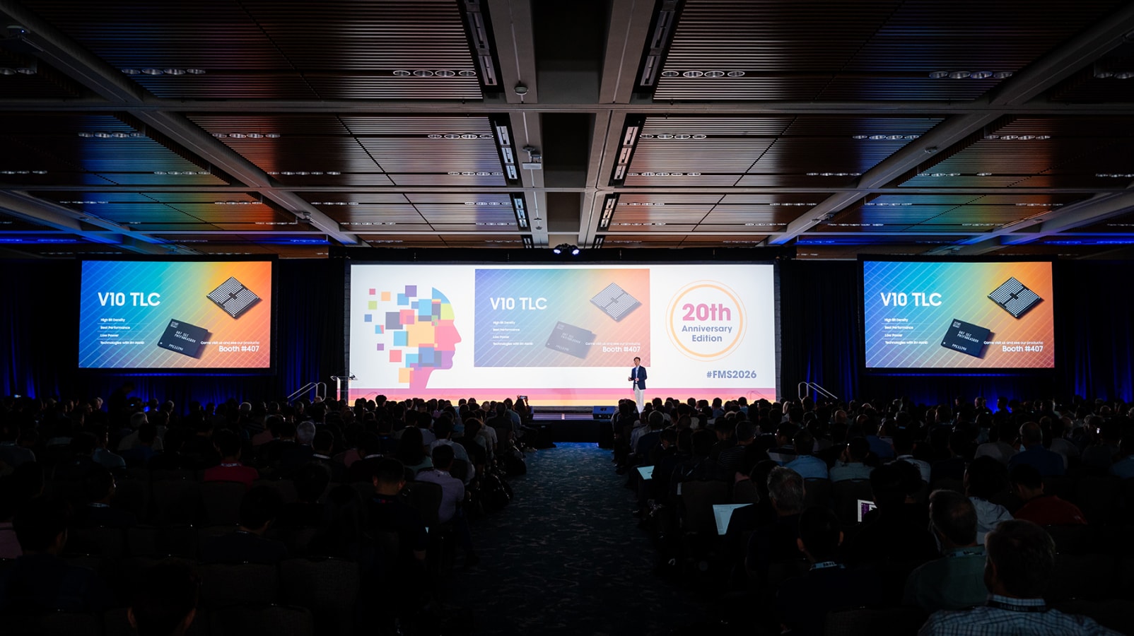
As AI continues to advance and the volume of data that needs to be processed grows exponentially, storage solutions are being called upon to deliver greater capacity, higher performance, and improved power efficiency. Against this backdrop, Samsung’s V10 BV-NAND received the 3D & NAND Innovation Award at the FMS 2026 Best of Show Awards, in recognition of its technological advancements in next-generation NAND.
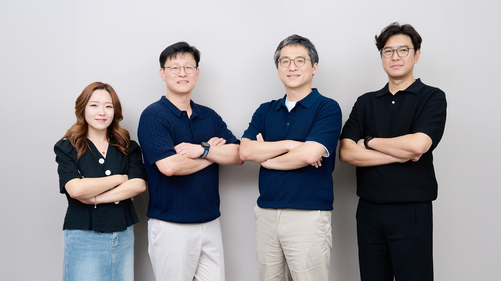
What market shifts and evolving customer needs inspired V10, and what technical challenges did the team overcome to bring it to life? We spoke with Byoung-Hee Kim and Jiyeon Shin from Product Planning, and Sangsoo Park and Dawoon Jeong from Development to learn more about the product’s development, its key technologies, and what the FMS 2026 award means to the team.
Q. Congratulations on winning the FMS 2026 3D & NAND Innovation Award. What is V10 BV-NAND, and what are the most notable advancements over the previous generation?
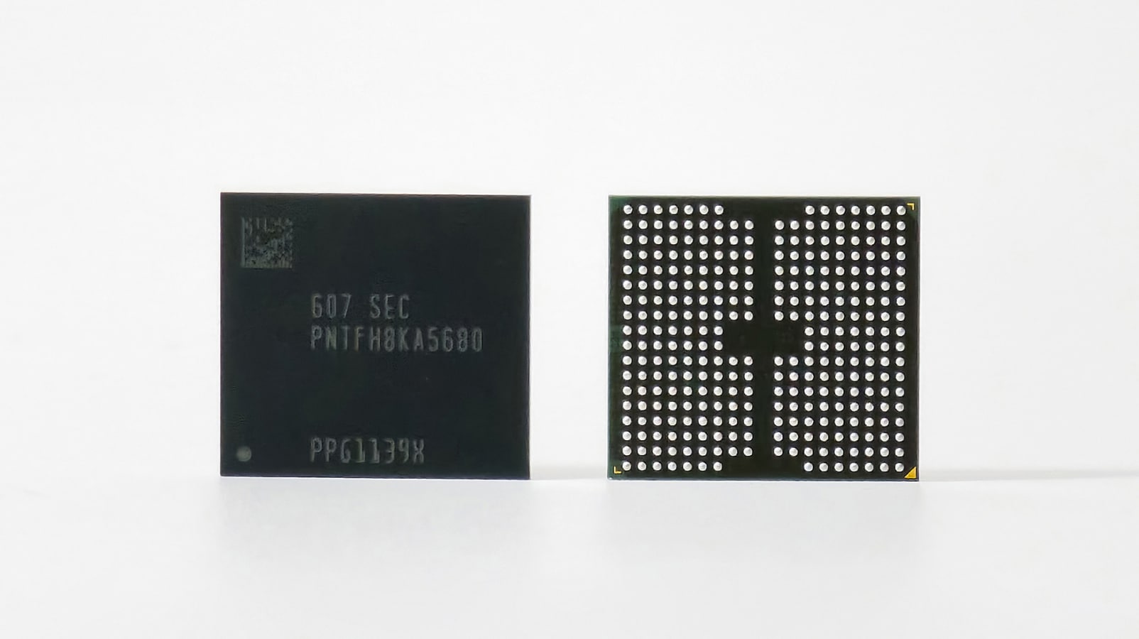
Jiyeon Shin: V10 is Samsung’s latest 3D NAND flash memory, developed to meet the growing demand for high-performance, high-capacity, and power-efficient storage in the AI era.
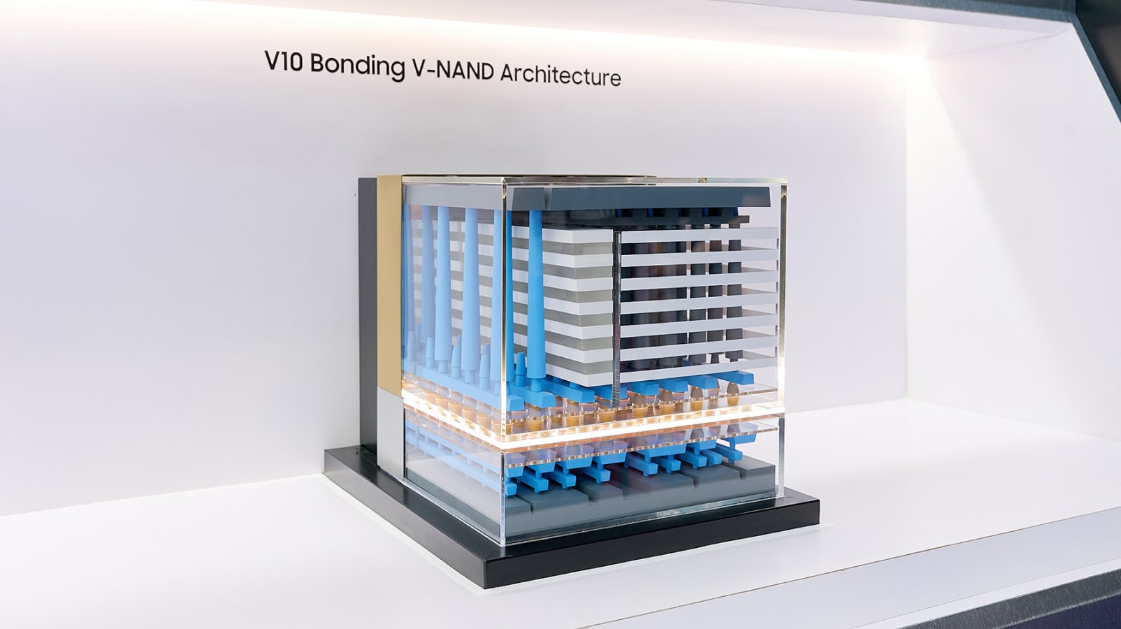
Based on Samsung’s 3D Bonded-VNAND architecture, V10 features more than 400 word lines (WL), achieving a more than 58% increase in bit density over the previous generation. It also delivers I/O speeds of more than 4.8Gbps, representing a performance improvement of over 33%, while reducing power consumption by more than 25%.
With these technological advancements, we expect V10 to become a key NAND solution for high-performance, high-capacity storage required by AI infrastructure, including ultra-high-capacity 128TB SSDs and next-generation PCIe Gen7 SSDs.
Q. As AI advances, the role of storage is also evolving rapidly. How did these market changes influence the product planning and development direction for V10?
Byoung-Hee Kim: With each generation, NAND flash has faced the challenge of increasing bit density while simultaneously improving performance and power efficiency. The rapid growth of AI workloads has made these requirements even more demanding.
As the volume of data generated and processed by AI systems continues to grow rapidly, storage solutions require greater capacity and higher I/O bandwidth. At the same time, power consumption has become a key factor in determining overall system efficiency and total cost of ownership (TCO) in data centers.
When planning V10, therefore, our goal was not simply to increase layer count or storage capacity. We set out to achieve higher density, higher performance, and lower power consumption simultaneously. An important objective was to provide a NAND solution capable of addressing expanding AI workloads across a wide range of applications, from data centers to PCs, mobile devices, and edge AI.
Q. What were the most important technological innovations in V10 that enabled the team to turn this product vision into reality?
Dawoon Jeong: The first major innovation was our advanced 3-stack HARC (High Aspect Ratio) Merge technology, which enabled a V-NAND architecture with more than 400 word lines.
As the number of V-NAND layers increases, the number of process steps, manufacturing costs, and process complexity can all increase as well. We developed HARC Merge technology to address these challenges. By combining it with Multi Hole and Zero Dummy Hole technologies, we achieved a 58% improvement in bit density over the previous generation while enhancing manufacturing efficiency and overall product quality.
The second major innovation was Wafer Bonding technology. We developed a process that separately fabricates the cell and peripheral (Peri) circuits on two wafers and then bonds them together. This enabled us to maximize the performance of the Peri devices and leverage their enhanced characteristics through circuit design to deliver both high performance and low power consumption.
Q. In addition to higher density, V10 delivers I/O speeds of more than 4.8Gbps, an improvement of over 33% compared to the previous generation. How was this performance improvement achieved?
Sangsoo Park: The 3D Bonded-VNAND architecture plays an important role not only in increasing density but also in improving I/O performance. By enabling low-temperature processing, we were able to scale the peripheral circuits, improve transistor characteristics, and enhance I/O performance.
We also introduced several innovations at the interface level. Samsung’s proprietary Pin-ODT technology enhances SCA (Separate Command and Address) operation, improving I/O efficiency by more than 75%.
In addition, we applied technologies such as DFE (Decision-Feedback Equalizer) and RDCA (Read-Duty-Cycle Adjustment) to mitigate ISI (Inter-Symbol Interference), which can occur during high-speed data transmission.
Together, these technologies enabled V10 to achieve I/O speeds of more than 4.8Gbps, providing the foundation to support the high I/O performance required by next-generation high-performance SSDs.
Q. Improving performance while reducing power consumption is a significant challenge. How did V10 achieve a power reduction of more than 25%?
Sangsoo Park: Improving power efficiency alongside performance was one of our key technical goals in developing V10.
First, we adopted a low-power circuit design that lowers the supply voltage (VCC) of the peripheral circuits and introduced an e-PIN architecture that directly utilizes external power sources. We also applied WL control techniques to reduce the power consumed in charging and discharging the word lines.
For high-speed I/O operation, we implemented PI-LTT (Power-Isolated Low-Tapped Termination), which lowers the channel voltage and further reduces power consumption at the interface.
By combining these low-power technologies, we were able to reduce power consumption by more than 25% compared to the previous generation. In high-capacity SSDs in particular, these improvements in NAND-level power efficiency can contribute to improved system-level power efficiency.
Q. What were the most difficult technical challenges in developing a highly integrated V-NAND with more than 400 layers, and how did you overcome them?
Sangsoo Park: Implementing a highly integrated 3D NAND flash memory with more than 400 layers was a demanding challenge that required us to overcome fundamental physical limitations, rather than simply increase the number of stacked layers.
The first challenge was extreme chip-size reduction. As the cell array becomes more highly integrated, the area required for the peripheral circuits that drive it inevitably increases. Designing the bottom peripheral circuitry to fit within the same footprint as the upper cell array was therefore extremely challenging.
To address this, we worked closely with design experts to develop a next-generation chip architecture optimized for the BV-NAND era. At the same time, we collaborated with our research teams to maximize process capabilities and tightly optimize the design rules to minimize transistor size. We also consolidated and optimized circuits with similar functions, ultimately achieving Full Capping, in which the bottom peripheral circuitry fits entirely within the footprint of the upper cell array.
The second challenge was the degradation of electrical characteristics as the number of word lines increases. As more layers are stacked, word-line capacitance increases, which can lead to higher power consumption, lower performance, and degradation in cell reliability.
We identified this as a critical issue for the continued scaling of high-layer-count NAND and began intensive research early in the development process. As a result, we developed a design technique for precise Multi-Stack control, reducing the voltage applied to the word lines of non-selected stacks during write operations by more than 70%. This significantly improved power efficiency while also delivering a 4% improvement in bit error rate (BER).
Dawoon Jeong: Developing NAND flash with more than 400 layers required us to overcome several major physical barriers through technological innovation.
One of the biggest challenges was wafer warpage caused by film stress, which became particularly difficult as V10 dramatically increased the number of layers. Conventional approaches used in previous generations had clear limitations, so engineers across the eight major process areas and process integration teams came together to develop new solutions. By introducing new processes and materials, overcoming equipment limitations, and optimizing the overall thermal budget, we significantly reduced wafer stress and overcame these physical constraints.
Another major concern from the early stages of R&D was cell reliability as channel lengths increased with the taller stack. To address this, we set ambitious targets for each process from the research stage and optimized the device accordingly, ultimately achieving a high level of reliability for mass production.
The Etch team optimized channel-hole profiles and variation for high reliability, while the Diffusion team secured the required step coverage and film characteristics even with taller stacks. The Cleaning team developed new technology to ensure uniform etching despite the increased surface area, while the PA team worked with the eight major process areas to optimize overall process integration and device design with cell reliability as a key priority.
As a result, we achieved our final reliability targets ahead of schedule and continued to develop the ideas generated throughout the process, enabling V10 to achieve a high level of cell reliability.
Q. V10 brings together technologies that were previously developed independently. How did teams across the organization collaborate during the development process?
Dawoon Jeong: Developing V10 was a process in which hundreds of engineers came together every day to discuss challenges and solve problems. HARC Merge and Wafer Bonding, two of the core technologies behind V-NAND, involve integrating module processes that had previously been developed independently and bonding two separately fabricated wafers into one.
As previously independent technologies became more tightly integrated, we encountered more defects involving complex interactions among multiple technologies. Overcoming these issues required close collaboration among engineers across different process areas, as well as a deeper understanding of one another’s work.
We had to go beyond our individual responsibilities and understand adjacent areas in order to solve problems together, which required extensive communication and collaboration across teams. We created cross-functional task-force meetings to give engineers more opportunities to discuss issues together, while broader interaction across teams helped deepen mutual understanding.
It was a valuable experience to see that as our culture of collaboration grew stronger, both product quality and our collective understanding of the new processes improved.
Q. V10 can support 128TB SSDs and next-generation PCIe Gen7 SSDs. From the perspective of customers and AI infrastructure, what value do you expect these technological innovations to deliver?
Jiyeon Shin: As AI continues to advance, the volume of data that needs to be processed and stored will continue to grow rapidly. In AI infrastructure in particular, massive amounts of data need to be stored and processed quickly, making storage capacity and performance increasingly important to overall system efficiency.
With its high bit density, V10 can support ultra-high-capacity 128TB SSDs, while its I/O performance of more than 4.8Gbps supports next-generation PCIe Gen7 SSDs. At the same time, improved power efficiency can help reduce power consumption and TCO in large-scale AI data centers.
Ultimately, V10’s technological innovations go beyond improving the performance of NAND itself. Their significance lies in delivering tangible customer value by simultaneously improving the capacity, performance, and power efficiency required by AI infrastructure.
Q. Finally, what does winning the FMS 2026 3D & NAND Innovation Award mean to the team? And where do you see V-NAND heading next?
Byoung-Hee Kim: Winning the FMS 2026 3D & NAND Innovation Award is particularly meaningful because it recognizes both the technological and product value of V10, as well as the direction we believe NAND needs to take in the AI era.
As AI continues to evolve, the capacity, performance, and power-efficiency requirements placed on storage will continue to rise. Samsung will continue to strengthen the competitiveness of V-NAND based on evolving market and customer needs, creating new value for next-generation AI storage.
Dawoon Jeong: V10 represents a significant step beyond the typical generational improvements in bit density, reliability, performance, and power efficiency. We set ambitious goals and established a clear direction from the early research stage, and hundreds of engineers worked closely together during product development to bring V10 to mass-production readiness.
As someone who participated in its development, I find it deeply rewarding that the FMS 2026 award recognizes V10’s technology on a global stage.
We often say that successful semiconductor development depends on everyone working together. There were difficult periods during V10 development as we pursued ambitious targets and encountered a wide range of issues arising from the increasing interdependence of technologies. That makes this recognition especially meaningful, as it reflects the effort of everyone who came together day after day to discuss and solve those challenges.
We also received tremendous support from teams across Samsung during the development of V10. Our manufacturing teams helped prioritize development lots and shorten turnaround times (TAT), while the introduction of Bonding technology to NAND flash benefited from existing Bonding infrastructure and technical expertise within our CIS organization. As the number of layers increased and the volume of FAB data grew, support from the A-FAB Technical Team’s YES organization also enabled our engineers to systematically analyze data and address defects.
It was this company-wide collaboration that enabled us to bring V10 to where it is today.
Sangsoo Park: This award is especially meaningful because it recognizes our ability to simultaneously address three major challenges of the AI era — higher density, higher performance, and lower power consumption — through Samsung’s differentiated technological capabilities.
Throughout the evolution of NAND flash, increasing density while maintaining high performance and low power has always involved difficult trade-offs. V10 became a reality because engineers across our research and development teams relentlessly pursued goals that once seemed impossible, through countless discussions and persistent problem-solving. The close collaboration among teams that worked as one to identify and resolve defects and reliability issues was also a major driving force behind this achievement.
The direction for V-NAND is clear. It must evolve beyond simply increasing capacity to become a core infrastructure technology that helps alleviate system bottlenecks and improve overall system efficiency in the AI era. Together with our colleagues, we will continue to push beyond physical limitations through technological innovation and strengthen our technology leadership to support a faster and more sustainable global AI ecosystem.
V10 BV-NAND combines an ultra-high-density architecture of more than 400 layers with higher performance and improved power efficiency, opening up new possibilities for storage in the AI era. Recognized with the FMS 2026 3D & NAND Innovation Award for its technological advancements, Samsung’s V10 is expected to help drive the evolution of AI infrastructure by enabling high-performance, high-capacity storage solutions including 128TB SSDs and next-generation PCIe Gen7 SSDs.

 Global