▲(Let to right) Lee Yong Gi, Noh Mi Jeong, Choi Yun Hyeok, and Kim Yong Su of the Foundry Business Division at Samsung Electronics’ DS Division
A solution for security-critical products In the age of the Quaternary Industrial Revolution, massive amounts of data are generated and transmitted through the Internet of Things (IoT) and the Cloud. With this staggering data volume, the importance of security technologies is ever-increasing. The security solution research engineers at the ASIC&IP Development Team in Samsung Electronics’ Foundry Business Division are a proud and committed bunch standing at the vanguard of semiconductor security technology. The team recognized the importance of PUF technology as a next-generation security solution early on. While there was abundant academic research on PUF, reliability was still insufficient for use in mass production. However, the engineers were confident that Samsung’s semiconductor technology and security know-how held the keys to a solution. Thus, their journey to hone PUF technology for mass production began.
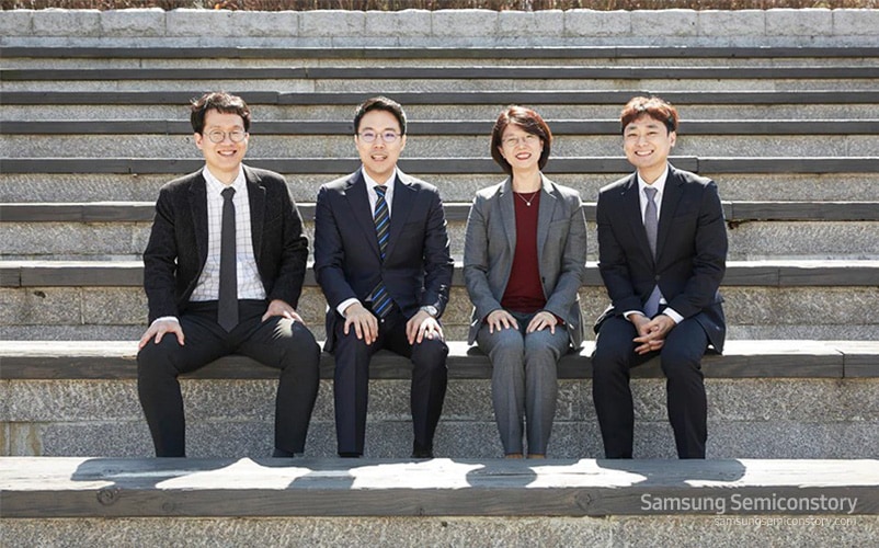
▲(Left to right) Noh Mi Jeong and Choi Yun Hyeok of the ASIC&IP Development Team in the Foundry Business Division at Samsung Electronics’ DS Division
Engineer Noh Mi Jeong of the Foundry Business Division’s ASIC&IP Development Team noted the extensive ‘trial and error’ runs the task involved; working with PUF technology requires an entirely different approach from that of conventional semiconductor design. “PUF technology maximizes minute physical variations that occur during semiconductor processes to generate a “chip fingerprint”. Paradoxically, “minimizing” variability is crucial for semiconductor fabrication, and characterizing processes in a manner suitable for PUF designs was quite the challenge. We also had to work with “randomness” in the values generated for each chip, as well as “stability” to ensure values would not change under temperature, voltage, and other environmental fluctuations once determined. Developing ideas to overcome these compound issues was an endless process of discussion, analysis, and simulation with our fellow researchers across all related fields. And once a design method was proven in theory, the method was applied to test chip fabrication and evaluated under varied conditions. This process was repeated countless times.” Until then, PUF technology had only existed in academic papers. Refining the technology for mass production naturally called for extensive effort. It was only after 50 months of PUF R&D since 2012 that the SAMPUF™ technology was completed.※ SAMPUF™: A trademark for Samsung Electronics’ PUF technology. SAMPUF™ can be applied to a variety of semiconductor processes, and provides both high randomness (the ability to generate a consecutive series of arbitrary numbers having no specific arrangement or rules) and high reliability for enhanced product security.
▲(Left to right) The brains behind the “SAMPUF™” semiconductor security technology. Lee Yong Gi, Noh Mi Jeong and Choi Yun Hyeok of the ASIC&IP Development Team in the Foundry Business Division at Samsung Electronics’ DS Division
Samsung Electronics’ SAMPUF™ paper was submitted to the 2016 ISSCC (International Solid-State Circuits Conference; the semiconductor world’s most prestigious academic society), promoting the excellence of the technology to semiconductor experts and scholars the world over. SAMPUF™ fingerprint security technology for semiconductors wins the IR52 Jang Young-shil Award for Technological Innovation
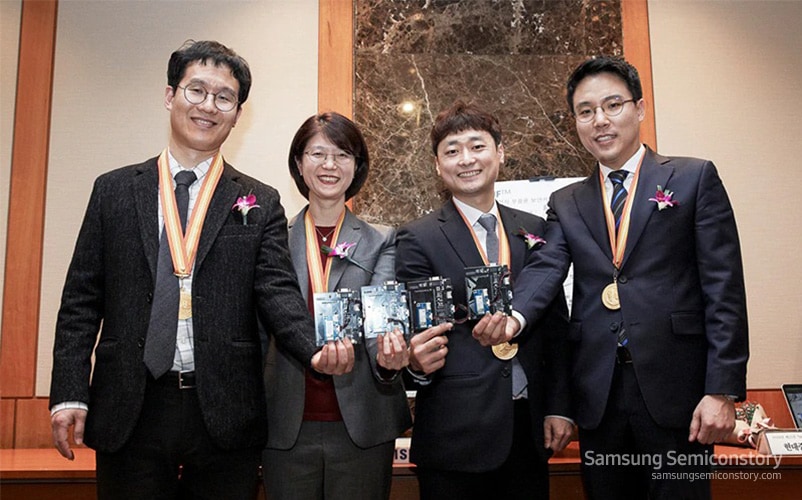
▲ Executive Vice President and Foundry Business Division’s ASIC&IP Development Team Leader Park Jaehong accepting the 2018 ‘‘IR52 Jang Young-shil Award for Technological Innovation’
Many obstacles were overcome in the development of Samsung Electronics’ SAMPUF™ technology. In recognition, the technology was conferred the honor of the “IR52 Jang Young-shil Award for Technological Innovation”, Korea’s most prestigious industrial R&D award, on March 16th.※ The IR52 Jang Young-shil Award for Technological Innovation: The Jang Young-shil award is given to 52 industrial research achievements annually, one for every week of the year (hence, “IR52”). The award recognizes the leading science and technology achievements powering the progress of Korean industrial technology.
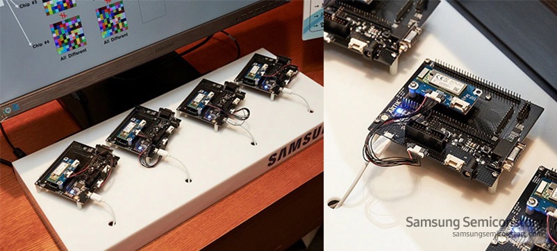
▲ Products incorporating Samsung Electronics’ 2018 IR52 Jang Young-shil Award-winning ‘SAMPUF™’ technology
Chips using advanced SAMPUF™ semiconductor chip security technology are fundamentally impossible to clone. This is true even for the developers of SAMPUF™ technology themselves, who know the technology in and out. The characteristics obtained in the process of manufacturing a semiconductor chip are impossible to fully replicate, meaning no cloned chip can have the same PUF output as the original. SAMPUF™ was first used in Samsung Electronics “Exynos iT200” IoT processor released in June of last year. The unique semiconductor security technology will find its way into diverse security-critical applications including IoT, mobile devices, and automobiles. “We have overcome countless obstacles so far, and in the same spirit we will continue to develop new and improved security solutions.” Engineer Noh Mi Jeong of the ASIC&IP Development Team in the Foundry Business Division at Samsung Electronics wanted to thank her colleagues for their perseverance, and the company for its patience during the protracted development process.” “I’m proud of our team for having been so tenacious; in the end, we ended up completing a technology few thought possible. It was the belief that we could do it that kept us going through all the hardships. SAMPUF™ was a great achievement. However, rather than rest on our laurels, we intend to jump right back into the game, developing the next generation of semiconductor security technologies to assert our global semiconductor technology leadership.”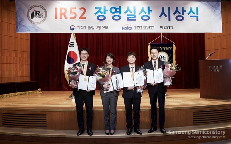
Registration Are you sure you want to submit this?
Your subscription is not active yet!
An email with an activation link
has just been sent to your email address.
Please activate your subscription by clicking on
the activation link inside the email.
You have already registered, but before we can send you the
information about upcoming events, we need your confirmation.
If you missed our previous email, please use the button below to resend it.
To activate your subscription, please click on the link included in the email.
